Part 1: Development Board Introduction
Here is a brief introduction to the functionality of the Kintex Ultrascale+ AXKU15 development platform.
The whole structure of the development board is designed by inheriting our consistent SOM module + expansion
board model. High-speed inter-board connectors are used between the module and the expansion board.
The module is mainly composed of XCKU15PFFVE1517 + 5 DDR4 + QSPI FLASH minimum systems. Using Xilinx's
Kintex Ultrascale+ series chip, model XCKU15PFFVE1517. Five DDR4 memory chips are connected to the HP port of
the FPGA chip. The capacity of each DDR4 chip is up to 1GB bytes, forming a data bit width of 80 bits. Two 512Mb
QSPI FLASHs are used to statically store configuration files or other user data of the FPGA chip.
The base board expands abundant peripheral interfaces for the module, including one PCIe3.0x16 interface, two
FMC HPC interfaces, one gigabit network interface, two MIPI input interfaces, one UART serial interface, one SD
card interface, and some keys and LEDs.
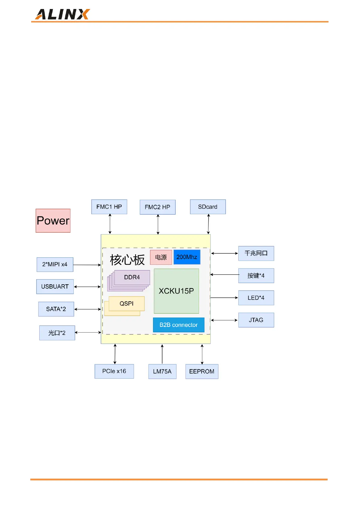
The following Figure 2 shows the structure of the entire development system:
Figure 2: Structure of AXKU15
Through this diagram, we can see the interfaces and functions that our development platform can contain.
⚫ FPGA SOM module
It is composed of the minimum system of XCKU15P + 5 DDR4 + 2 QSPI FLASH. In addition, two crystal oscillators
provide the clock, and two 200MHz crystal oscillators provide the reference clock for FPGA logic and DDR control.