Table of Contents
Version Record .................................................................................................................................. 2
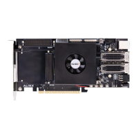
Part 1: Development Board Introduction ................................................................................... 5
Part 2: ACKU15 SOM Module ........................................................................................................ 7
Part 2.1: Introduction ............................................................................................................... 7
Part 2.2: FPGA Chip.................................................................................................................. 7
Part 2.3: DDR4 ........................................................................................................................... 9
Part 2.4: QSPI Flash ............................................................................................................... 13
Part 2.5: Clock Configuration ............................................................................................. 14
Part 2.6: LED Light ................................................................................................................. 15
Part 2.7: Power source ......................................................................................................... 16
Part 2.8: Structure Diagram ................................................................................................ 17
Part 2.9: Connector pin definition .................................................................................... 17
Part 3: Base board ......................................................................................................................... 29
Part 3.1: Introduction ............................................................................................................ 29
Part 3.2: PCIe Slot .................................................................................................................. 29
Part 3.3: Gigabit network interface .................................................................................. 31
Part 3.4: FMC HPC Interface ............................................................................................... 33
Part 3.5: MIPI Interface ........................................................................................................ 41
Part 3.6: USB To serial port ................................................................................................. 42
Part 3.7: SD Card slot ........................................................................................................... 43
Part 3.8: SATA Interface ....................................................................................................... 44
Part 3.9: Keys and LED Light ............................................................................................... 45
Part 3.10: EEPROM................................................................................................................. 45
Part 3.11: Temperature sensor ............................................................................................ 46
Part 3.12: Fiber Optic Interface .......................................................................................... 47
Part 3.13: JTAG Debugging port ........................................................................................ 49
Part 3.14: Power source ........................................................................................................ 49
Part 3.14: Structural dimension drawing ......................................................................... 51