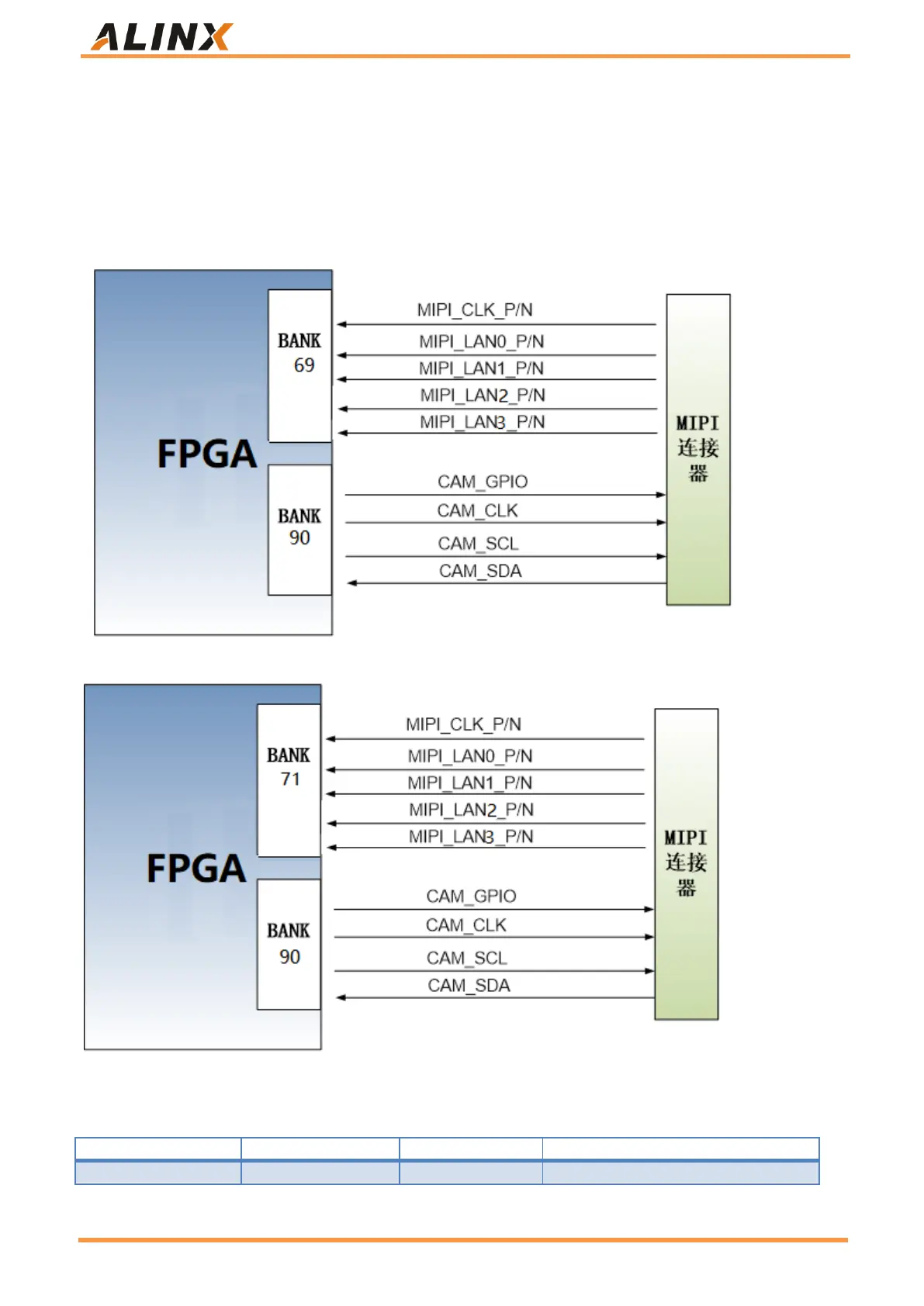
Part 3.5: MIPI Interface
The AXKU15 base board is equipped with two MIPI lanex4 camera input interfaces. MIPI1 corresponds to J9 and is
connected to BANK69 and BANK90 of FPGA. MIPI2 corresponds to J10, and is connected to BANK66 and BANK84
of FPGA, and is connected to BANK71 and BANK90 of FPGA. The design schematic diagram of connection is
shown in Figure 21 and 22 below:
Figure 21: Schematic diagram of MIPI1 interface design
Figure 22: Schematic diagram of MIPI2 interface design
MIPI1 interface pin assignment:
 Loading...