Part 2.4: QSPI Flash
The module is equipped with two Quad-SPI FLASH chips of 512MBit size, model MT25QU512ABA1EW9, which uses
1.8V CMOS voltage standard. Due to the non-volatile nature of QSPI FLASH, it can store the configuration Bin file
of the FPGA as well as other user data files during use. See Table 4 for the specific model and relevant parameters
of QSPI FLASH.
Table 4: Model and Parameters of QSPI Flash
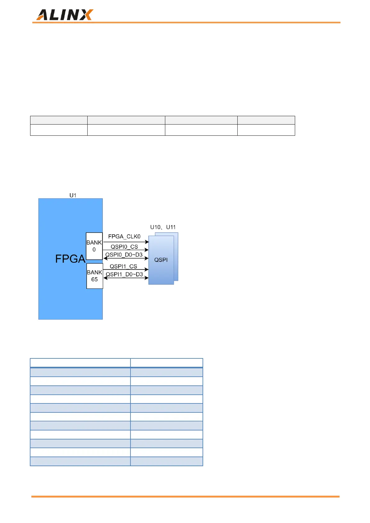
The QSPI FLASH is connected to a dedicated pin of the FPGA chip, wherein the clock pin is connected to CCLK0 of
the dedicated BANK0, and the data pins are respectively connected to BANK0 and BANK65. Figure 8 is the
connection diagram of QSPI Flash and FPGA chip.
Figure 8: QSPI Flash Connection Diagram
Configure chip pin assignment:
 Loading...