www.en.alinx.com
www.en.alinx.com
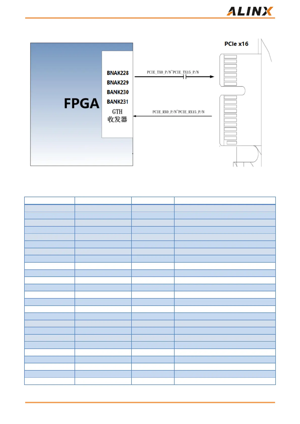
Figure 16: Schematic Diagram of PCIe Slot Design
The PCIe x16 interface FPGA pin assignments are as follows:
PCIE channel 0 data receiving positive
PCIE Channel 0 Data Receive Negative
PCIE channel 1 data receiving positive
PCIE Channel 1 Data Receive Negative
PCIE channel 2 data receiving positive
PCIE Channel 2 Data Receive Negative
PCIE channel 3 data receiving positive
PCIE Channel 3 Data Receive Negative
PCIE Channel 4 Data Reception Positive
PCIE Channel 4 Data Receive Negative
PCIE channel 5 data receiving positive
PCIE Channel 5 Data Receive Negative
PCIE channel 6 data receiving positive
PCIE Channel 6 Data Receive Negative
PCIE channel 7 data receiving positive
PCIE Channel 7 Data Receive Negative
PCIE Channel 8 Data Sending Positive
PCIE channel 8 data transmission negative
PCIE Channel 9 Data Sending Positive
PCIE channel 9 data transmission negative
PCIE Channel 10 Data Sending Positive
PCIE channel 10 data transmission negative
PCIE Channel 11 Data Sending Positive
PCIE channel 11 data transmission negative
PCIE Channel 12 Data Sending Positive
 Loading...