Page 32
Features & Functionality
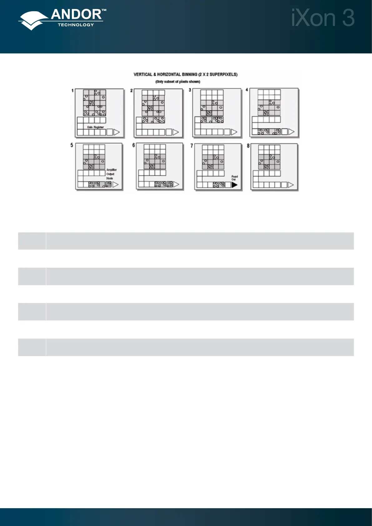
Step 1 Charge is built up on the sensor
Step 2 Charge in the frame is shifted vertically by one row, so that the bottom row of charge moves down into the shift register.
Step 3
Charge in the frame is shifted vertically by a further row, so that the next row of charge moves down into the shift register, which now
contains charge from two rows - i.e. the charge is vertically binned.
Step 4
Charge in the shift register is moved horizontally (through the EM gain register, if using the EM output amplier) until the rst data pixel is just
about to enter the output node of the amplier.
Step 5
Charge in the shift / EM gain register is moved horizontally by one pixel, so that charge on the endmost pixel of the shift register is transferred
into the output node of the amplier
Step 6
Charge in the shift register is again moved horizontally, so that the output node of the amplier now contains charge from two pixels of the
shift register - i.e. the charge has been horizontally binned.
Step 7 The charge in the output node of the amplier is passed to the analog-to-digital converter and is read out
Step 8 Steps 5 - 7 are repeated until the shift register is empty. The process is repeated from Step 2 until the whole frame is read out.
Figure 21: Vertical & Horizontal binning of two rows
 Loading...