Page 69
APPENDIX
A1.1.- GLOSSARY
If this is the rst time you have used Andor’s EMCCD, the glossary that follows will help familiarize you with its design
philosophy and some of its key terminology.
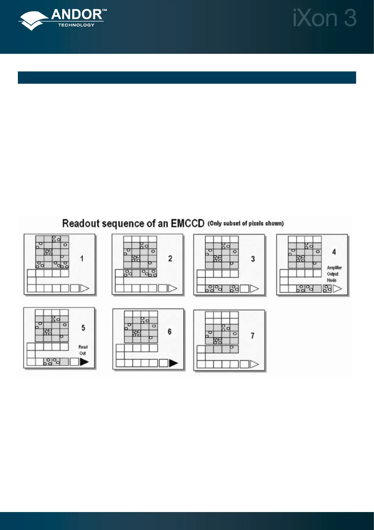
A1.1.1 - Readout sequence of an EMCCD
In the course of readout, charge is moved vertically into the shift register then horizontally from the shift register into the
output node of the amplier. The simple readout sequence illustrated below (which corresponds to the default setting
of the Full Resolution Image binning pattern) allows data to be recorded for each individual element on
theEMCCD-chip.Otherbinningpatternsareachievedbysummingchargeintheshiftregisterand/ortheoutputnode
prior to readout. For further information on Binning, please refer to pages 41 - 42).
1. Exposure to light causes a pattern of charge (an electronic image) to build up on the frame (or Image Area) of the
EMCCD-chip.
2. Charge in the frame is shifted vertically by one row, so that the bottom row of charge moves into the shift register.
3. Charge in the shift register is moved horizontally by one pixel, so that charge on the endmost pixel of the shift
register is moved into the Gain register.
4. Charge is shifted into the output node of the amplier.
5. The charge in the output node of the amplier is passed to the analog-to-digital converter and is read out.
6. Steps 3 and 4 are repeated until the shift register is emptied of charge.
7. The frame is shifted vertically again, so that the next row of charge moves down into the shift register.
The process is repeated from Step 3 until the whole frame is read out.
Appendix
 Loading...