266
8025I–AVR–02/09
ATmega48P/88P/168P/328P
trigger signal. If ADEN in ADCSRA is set, this will start a conversion. Switching to Free Running
mode (ADTS[2:0]=0) will not cause a trigger event, even if the ADC Interrupt Flag is set
.
21.9.5 DIDR0 – Digital Input Disable Register 0
• Bits 7:6 – Res: Reserved Bits
These bits are reserved for future use. To ensure compatibility with future devices, these bits
must be written to zero when DIDR0 is written.
• Bit 5:0 – ADC5D..ADC0D: ADC5..0 Digital Input Disable
When this bit is written logic one, the digital input buffer on the corresponding ADC pin is dis-
abled. The corresponding PIN Register bit will always read as zero when this bit is set. When an
analog signal is applied to the ADC5..0 pin and the digital input from this pin is not needed, this
bit should be written logic one to reduce power consumption in the digital input buffer.
Note that ADC pins ADC7 and ADC6 do not have digital input buffers, and therefore do not
require Digital Input Disable bits.
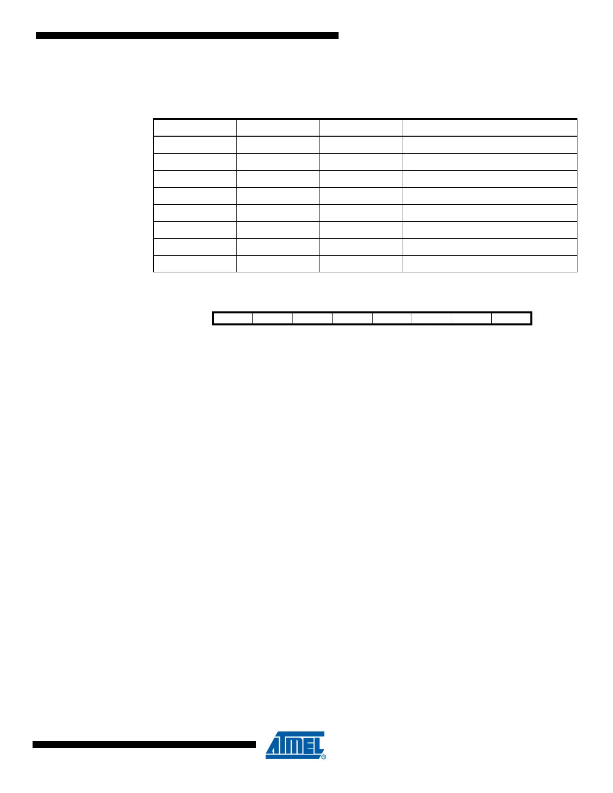
Table 21-6. ADC Auto Trigger Source Selections
ADTS2 ADTS1 ADTS0 Trigger Source
0 0 0 Free Running mode
0 0 1 Analog Comparator
0 1 0 External Interrupt Request 0
0 1 1 Timer/Counter0 Compare Match A
1 0 0 Timer/Counter0 Overflow
1 0 1 Timer/Counter1 Compare Match B
1 1 0 Timer/Counter1 Overflow
1 1 1 Timer/Counter1 Capture Event
Bit 76543210
(0x7E) – – ADC5D ADC4D ADC3D ADC2D ADC1D ADC0D DIDR0
Read/Write R R R/W R/W R/W R/W R/W R/W
Initial Value 0 0 0 0 0 0 0 0