EasyManua.ls Logo

Atmel ATtiny25 User Manual

Atmel ATtiny25
196 pages
To Next Page IconTo Next Page
To Previous Page IconTo Previous Page
Page #107 background imageLoading...
Page #107 background image
107
7598H–AVR–07/09
ATtiny25/45/85
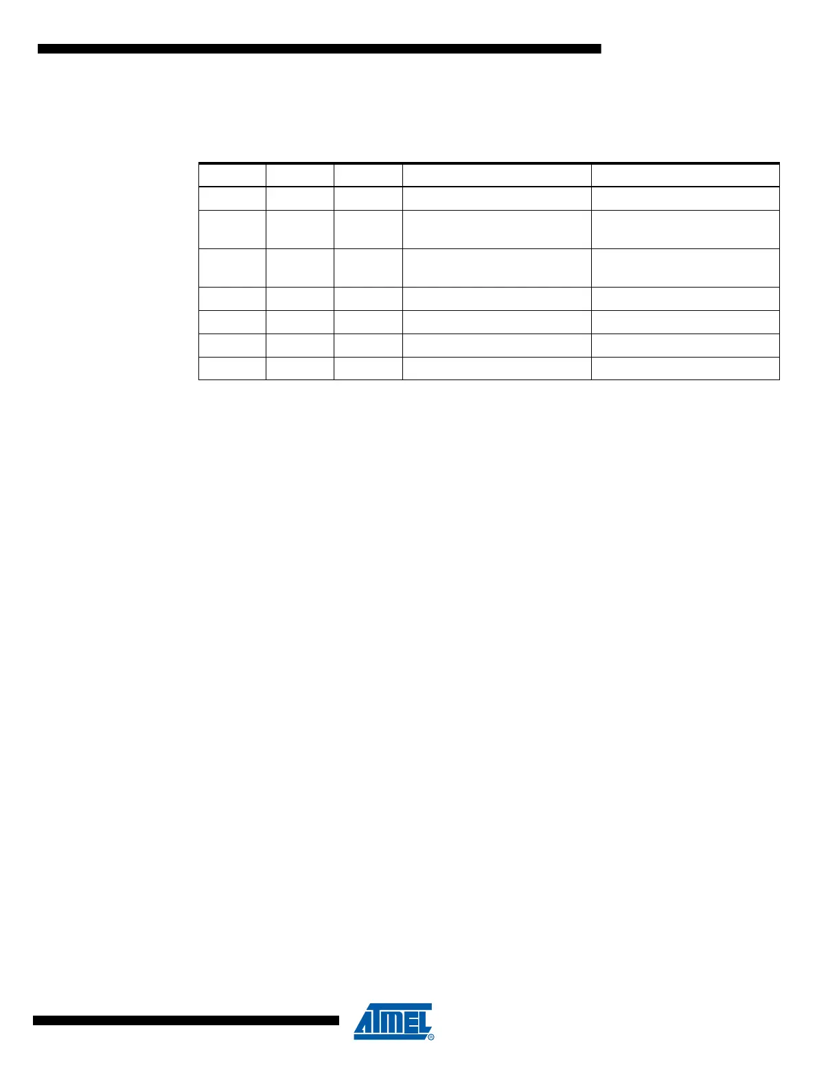
Table 16-2 shows the relationship between the USICS1..0 and USICLK setting and clock source
used for the Shift Register and the 4-bit counter.
Bit 1 – USICLK: Clock Strobe
Writing a one to this bit location strobes the Shift Register to shift one step and the counter to
increment by one, provided that the USICS1..0 bits are set to zero and by doing so the software
clock strobe option is selected. The output will change immediately when the clock strobe is exe-
cuted, i.e., in the same instruction cycle. The value shifted into the Shift Register is sampled the
previous instruction cycle. The bit will be read as zero.
When an external clock source is selected (USICS1 = 1), the USICLK function is changed from
a clock strobe to a Clock Select Register. Setting the USICLK bit in this case will select the
USITC strobe bit as clock source for the 4-bit counter (see Table 16-2).
Bit 0 – USITC: Toggle Clock Port Pin
Writing a one to this bit location toggles the USCK/SCL value either from 0 to 1, or from 1 to 0.
The toggling is independent of the setting in the Data Direction Register, but if the PORT value is
to be shown on the pin the DDRE4 must be set as output (to one). This feature allows easy clock
generation when implementing master devices. The bit will be read as zero.
When an external clock source is selected (USICS1 = 1) and the USICLK bit is set to one, writ-
ing to the USITC strobe bit will directly clock the 4-bit counter. This allows an early detection of
when the transfer is done when operating as a master device.
Table 16-2. Relations between the USICS1..0 and USICLK Setting
USICS1 USICS0 USICLK Shift Register Clock Source 4-bit Counter Clock Source
0 0 0 No Clock No Clock
001
Software clock strobe
(USICLK)
Software clock strobe
(USICLK)
01X
Timer/Counter0 Compare
Match
Timer/Counter0 Compare
Match
1 0 0 External, positive edge External, both edges
1 1 0 External, negative edge External, both edges
1 0 1 External, positive edge Software clock strobe (USITC)
1 1 1 External, negative edge Software clock strobe (USITC)

Table of Contents

Question and Answer IconNeed help?

Do you have a question about the Atmel ATtiny25 and is the answer not in the manual?

Atmel ATtiny25 Specifications

General IconGeneral
ArchitectureAVR
Flash Memory2 KB
SRAM128 B
EEPROM128 B
Clock Speed20 MHz
I/O Pins6
PWM Channels2
Operating Voltage1.8V - 5.5V
ADC4 channels, 10-bit
Communication InterfacesSPI, I2C, USART
Operating Temperature Range-40°C to 85°C
Timers8-bit Timer/Counter with PWM, 16-bit Timer/Counter with PWM
Package8-pin PDIP, SOIC-8

Summary

Features

Overview and Pin Configurations

Pinout

Pin configuration details for ATtiny25/45/85, showing pin functions for SOIC and QFN packages.

Overview

Introduces the ATtiny25/45/85 as a low-power AVR microcontroller with RISC architecture.

AVR CPU Core

Architecture & Registers

Covers CPU core, architectural overview, ALU, status, and general purpose registers.

Instruction Execution & Reset/Interrupts

Details instruction timing, reset, and interrupt handling mechanisms.

ATtiny25/45/85 Memories

Flash, SRAM, EEPROM, and I/O Memory

Describes Flash, SRAM, EEPROM, and I/O memory spaces and their characteristics.

System Clock and Clock Options

Clock Sources and Prescalers

Details clock sources (RC, Crystal, PLL) and the system clock prescaler.

Power Management and Sleep Modes

MCU Control Register

Details the MCU Control Register for power management and sleep mode selection.

Sleep Modes (Idle, ADC Noise Reduction, Power-down)

Explains the different sleep modes and their features for power saving.

Power Reduction Register

Describes the PRR for stopping clocks to peripherals to reduce power consumption.

System Control and Reset

Reset Sources

Lists and describes the various reset sources like Power-on, External, Watchdog, and Brown-out.

Brown-out Detection

Details the On-chip Brown-out Detection (BOD) circuit and its configuration.

Interrupts

Interrupt Vectors in ATtiny25/45/85

Lists the interrupt vectors and their definitions for ATtiny25/45/85.

I/O Ports

Ports as General Digital I/O

Covers port configuration, general I/O, and switching between input/output.

Alternate Port Functions

Explains alternate functions of port pins and overriding signals.

Register Description for I/O-Ports

Details the PORTB, DDRB, and PINB registers for I/O port control.

External Interrupts

MCU Control Register – MCUCR

Details the External Interrupt Control Register for interrupt sense control.

General Interrupt Mask Register – GIMSK

Covers the GIMSK for enabling external and pin change interrupts.

8-bit Timer/Counter0 with PWM

Modes of Operation and Registers

Explains operational modes and register descriptions for Timer/Counter0.

Counter and Compare Units

Timer/Counter1 and Dead Time Generator

Details Timer/Counter1 operation and the Dead Time Generator for PWM.

Universal Serial Interface – USI

Functional Descriptions and Registers

Covers USI modes (3-wire, SPI, 2-wire) and register descriptions.

Analog Comparator

ACSR and ADCSRB Registers

Details Analog Comparator Control and Status Registers for configuration and interrupts.

Analog Comparator Multiplexed Input

Explains selecting ADC pins as the negative input to the Analog Comparator.

Analog to Digital Converter

ADC Features and Operation

Lists ADC features and describes its operation, including channel and reference selection.

Starting a Conversion

Explains manual and auto-triggered ADC conversion start methods.

ADC Conversion Result

Details how to read and interpret ADC conversion results in different modes.

debugWIRE On-chip Debug System

Features, Interface, and Registers

Covers debugwire features, physical interface, limitations, and registers.

Memory Programming

Lock Bits and Fuse Bytes

Explains memory lock bits and the functionality of fuse bytes.

Serial Downloading

Details serial programming methods including SPI and HVSP.

High-voltage Serial Programming

Covers programming Flash, EEPROM, Lock bits, and Fuse bits using HVSP.

Electrical Characteristics

Absolute Maximum Ratings*

Lists the stress ratings that may cause permanent damage to the device.

DC Characteristics

Provides DC characteristics across temperature and voltage ranges.

Typical Characteristics

Supply Current (Active, Idle, Power-down)

Shows supply current graphs for different modes versus frequency and VCC.

Pin Characteristics (Pull-up, Driver Strength, Thresholds)

Details pin pull-up, driver strength, and threshold characteristics.

Oscillator and BOD Characteristics

Covers BOD thresholds and internal oscillator frequency characteristics.

Register Summary

Instruction Set Summary

Ordering Information

Package Types

Lists available package types like T5 and PC with their specifications.

Document Revision History

Errata

Related product manuals