EasyManua.ls Logo

Atmel ATtiny25 User Manual

Atmel ATtiny25
196 pages
To Next Page IconTo Next Page
To Previous Page IconTo Previous Page
Page #126 background imageLoading...
Page #126 background image
126
7598H–AVR–07/09
ATtiny25/45/85
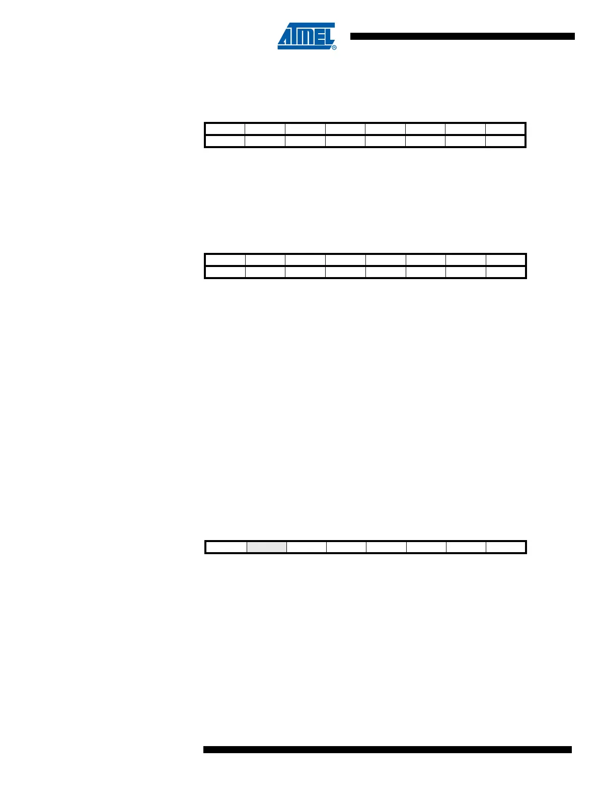
18.7.7 The ADC Data Register – ADCL and ADCH
18.7.7.1 ADLAR = 0
18.7.7.2 ADLAR = 1
When an ADC conversion is complete, the result is found in these two registers.
When ADCL is read, the ADC Data Register is not updated until ADCH is read. Consequently, if
the result is left adjusted and no more than 8-bit precision is required, it is sufficient to read
ADCH. Otherwise, ADCL must be read first, then ADCH.
The ADLAR bit in ADMUX, and the MUXn bits in ADMUX affect the way the result is read from
the registers. If ADLAR is set, the result is left adjusted. If ADLAR is cleared (default), the result
is right adjusted.
ADC9:0: ADC Conversion Result
These bits represent the result from the conversion, as detailed in “ADC Conversion Result” on
page 121.
18.7.8 ADC Control and Status Register B – ADCSRB
Bit 7– BIN: Bipolar Input Mode
The gain stage is working in the unipolar mode as default, but the bipolar mode can be selected
by writing the BIN bit in the ADCSRB register. In the unipolar mode only one-sided conversions
are supported and the voltage on the positive input must always be larger than the voltage on
the negative input. Otherwise the result is saturated to the voltage reference. In the bipolar mode
two-sided conversions are supported and the result is represented in the two’s complement
form. In the unipolar mode the resolution is 10 bits and the bipolar mode the resolution is 9 bits +
1 sign bit.
Bit 151413121110 9 8
ADC9 ADC8 ADCH
ADC7 ADC6 ADC5 ADC4 ADC3 ADC2 ADC1 ADC0 ADCL
76543210
Read/Write RRRRRRRR
RRRRRRRR
Initial Value 0 0 0 0 0 0 0 0
00000000
Bit 151413121110 9 8
ADC9 ADC8 ADC7 ADC6 ADC5 ADC4 ADC3 ADC2 ADCH
ADC1 ADC0 ADCL
76543210
Read/Write RRRRRRRR
RRRRRRRR
Initial Value 0 0 0 0 0 0 0 0
00000000
Bit 76543210
BIN
ACME IPR ADTS2 ADTS1 ADTS0 ADCSRB
Read/Write R/W R/W R/W R R R/W R/W R/W
Initial Value00000000

Table of Contents

Question and Answer IconNeed help?

Do you have a question about the Atmel ATtiny25 and is the answer not in the manual?

Atmel ATtiny25 Specifications

General IconGeneral
ArchitectureAVR
Flash Memory2 KB
SRAM128 B
EEPROM128 B
Clock Speed20 MHz
I/O Pins6
PWM Channels2
Operating Voltage1.8V - 5.5V
ADC4 channels, 10-bit
Communication InterfacesSPI, I2C, USART
Operating Temperature Range-40°C to 85°C
Timers8-bit Timer/Counter with PWM, 16-bit Timer/Counter with PWM
Package8-pin PDIP, SOIC-8

Summary

Features

Overview and Pin Configurations

Pinout

Pin configuration details for ATtiny25/45/85, showing pin functions for SOIC and QFN packages.

Overview

Introduces the ATtiny25/45/85 as a low-power AVR microcontroller with RISC architecture.

AVR CPU Core

Architecture & Registers

Covers CPU core, architectural overview, ALU, status, and general purpose registers.

Instruction Execution & Reset/Interrupts

Details instruction timing, reset, and interrupt handling mechanisms.

ATtiny25/45/85 Memories

Flash, SRAM, EEPROM, and I/O Memory

Describes Flash, SRAM, EEPROM, and I/O memory spaces and their characteristics.

System Clock and Clock Options

Clock Sources and Prescalers

Details clock sources (RC, Crystal, PLL) and the system clock prescaler.

Power Management and Sleep Modes

MCU Control Register

Details the MCU Control Register for power management and sleep mode selection.

Sleep Modes (Idle, ADC Noise Reduction, Power-down)

Explains the different sleep modes and their features for power saving.

Power Reduction Register

Describes the PRR for stopping clocks to peripherals to reduce power consumption.

System Control and Reset

Reset Sources

Lists and describes the various reset sources like Power-on, External, Watchdog, and Brown-out.

Brown-out Detection

Details the On-chip Brown-out Detection (BOD) circuit and its configuration.

Interrupts

Interrupt Vectors in ATtiny25/45/85

Lists the interrupt vectors and their definitions for ATtiny25/45/85.

I/O Ports

Ports as General Digital I/O

Covers port configuration, general I/O, and switching between input/output.

Alternate Port Functions

Explains alternate functions of port pins and overriding signals.

Register Description for I/O-Ports

Details the PORTB, DDRB, and PINB registers for I/O port control.

External Interrupts

MCU Control Register – MCUCR

Details the External Interrupt Control Register for interrupt sense control.

General Interrupt Mask Register – GIMSK

Covers the GIMSK for enabling external and pin change interrupts.

8-bit Timer/Counter0 with PWM

Modes of Operation and Registers

Explains operational modes and register descriptions for Timer/Counter0.

Counter and Compare Units

Timer/Counter1 and Dead Time Generator

Details Timer/Counter1 operation and the Dead Time Generator for PWM.

Universal Serial Interface – USI

Functional Descriptions and Registers

Covers USI modes (3-wire, SPI, 2-wire) and register descriptions.

Analog Comparator

ACSR and ADCSRB Registers

Details Analog Comparator Control and Status Registers for configuration and interrupts.

Analog Comparator Multiplexed Input

Explains selecting ADC pins as the negative input to the Analog Comparator.

Analog to Digital Converter

ADC Features and Operation

Lists ADC features and describes its operation, including channel and reference selection.

Starting a Conversion

Explains manual and auto-triggered ADC conversion start methods.

ADC Conversion Result

Details how to read and interpret ADC conversion results in different modes.

debugWIRE On-chip Debug System

Features, Interface, and Registers

Covers debugwire features, physical interface, limitations, and registers.

Memory Programming

Lock Bits and Fuse Bytes

Explains memory lock bits and the functionality of fuse bytes.

Serial Downloading

Details serial programming methods including SPI and HVSP.

High-voltage Serial Programming

Covers programming Flash, EEPROM, Lock bits, and Fuse bits using HVSP.

Electrical Characteristics

Absolute Maximum Ratings*

Lists the stress ratings that may cause permanent damage to the device.

DC Characteristics

Provides DC characteristics across temperature and voltage ranges.

Typical Characteristics

Supply Current (Active, Idle, Power-down)

Shows supply current graphs for different modes versus frequency and VCC.

Pin Characteristics (Pull-up, Driver Strength, Thresholds)

Details pin pull-up, driver strength, and threshold characteristics.

Oscillator and BOD Characteristics

Covers BOD thresholds and internal oscillator frequency characteristics.

Register Summary

Instruction Set Summary

Ordering Information

Package Types

Lists available package types like T5 and PC with their specifications.

Document Revision History

Errata

Related product manuals