140
7598H–AVR–07/09
ATtiny25/45/85
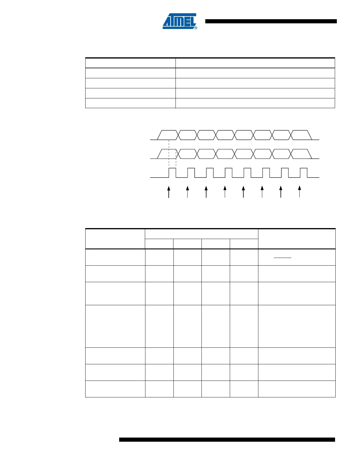
Figure 21-2. Serial Programming Waveforms
Table 21-9. Minimum Wait Delay Before Writing the Next Flash or EEPROM Location
Symbol Minimum Wait Delay
t
WD_FLASH
4.5 ms
t
WD_EEPROM
4.0 ms
t
WD_ERASE
4.0 ms
t
WD_FUSE
4.5 ms
Table 21-10. Serial Programming Instruction Set
Instruction
Instruction Format
OperationByte 1 Byte 2 Byte 3 Byte4
Programming Enable
1010
1100
0101
0011
xxxx
xxxx
xxxx
xxxx
Enable Serial Programming
after RESET
goes low.
Chip Erase
1010
1100
100x
xxxx
xxxx
xxxx
xxxx
xxxx
Chip Erase EEPROM and
Flash.
Read Program
Memory
0010
H000
0000
000a
bbbb
bbbb
oooo
oooo
Read H (high or low) data o
from Program memory at
word address a:b.
Load Program
Memory Page
0100
H000
000x
xxxx
xxxb
bbbb
iiii
iiii
Write H (high or low) data i to
Program memory page at
word address b. Data low
byte must be loaded before
Data high byte is applied
within the same address.
Write Program
Memory Page
0100
1100
0000
000a
bbxx
xxxx
xxxx
xxxx
Write Program memory Page
at address a:b.
Read EEPROM
Memory
1010
0000
000x
xxxx
xxbb
bbbb
oooo
oooo
Read data o from EEPROM
memory at address b.
Write EEPROM
Memory
1100
0000
000x
xxxx
xxbb
bbbb
iiii
iiii
Write data
i to EEPROM
memory at address b.
MSB
MSB
LSB
LSB
SERIAL CLOCK INPUT
(SCK)
SERIAL DATA INPUT
(MOSI)
(MISO)
SAMPLE
SERIAL DATA OUTPUT