98
7598H–AVR–07/09
ATtiny25/45/85
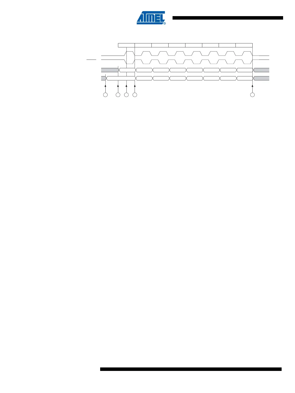
Figure 16-3. Three-wire Mode, Timing Diagram
The Three-wire mode timing is shown in Figure 16-3. At the top of the figure is a USCK cycle ref-
erence. One bit is shifted into the USI Shift Register (USIDR) for each of these cycles. The
USCK timing is shown for both external clock modes. In External Clock mode 0 (USICS0 = 0), DI
is sampled at positive edges, and DO is changed (Data Register is shifted by one) at negative
edges. External Clock mode 1 (USICS0 = 1) uses the opposite edges versus mode 0, i.e., sam-
ples data at negative and changes the output at positive edges. The USI clock modes
corresponds to the SPI data mode 0 and 1.
Referring to the timing diagram (Figure 16-3.), a bus transfer involves the following steps:
1. The Slave device and Master device sets up its data output and, depending on the pro-
tocol used, enables its output driver (mark A and B). The output is set up by writing the
data to be transmitted to the Serial Data Register. Enabling of the output is done by set-
ting the corresponding bit in the port Data Direction Register. Note that point A and B
does not have any specific order, but both must be at least one half USCK cycle before
point C where the data is sampled. This must be done to ensure that the data setup
requirement is satisfied. The 4-bit counter is reset to zero.
2. The Master generates a clock pulse by software toggling the USCK line twice (C and
D). The bit value on the slave and master’s data input (DI) pin is sampled by the USI on
the first edge (C), and the data output is changed on the opposite edge (D). The 4-bit
counter will count both edges.
3. Step 2. is repeated eight times for a complete register (byte) transfer.
4. After eight clock pulses (i.e., 16 clock edges) the counter will overflow and indicate that
the transfer is completed. The data bytes transferred must now be processed before a
new transfer can be initiated. The overflow interrupt will wake up the processor if it is set
to Idle mode. Depending of the protocol used the slave device can now set its output to
high impedance.
16.2.2 SPI Master Operation Example
The following code demonstrates how to use the USI module as a SPI Master:
SPITransfer:
sts USIDR,r16
ldi r16,(1<<USIOIF)
sts USISR,r16
ldi r16,(1<<USIWM0)|(1<<USICS1)|(1<<USICLK)|(1<<USITC)
SPITransfer_loop:
sts USICR,r16
lds r16, USISR
sbrs r16, USIOIF
MSB
MSB
654321LSB
1 2 3 4 5 6 7 8
654321LSB
USCK
USCK
DO
DI
DCBA E
CYCLE
( Reference )