367
7679H–CAN–08/08
AT90CAN32/64/128
Notes: 1. “Max” means the highest value where the pin is guaranteed to be read as low
2. “Min” means the lowest value where the pin is guaranteed to be read as high
3. Although each I/O port can sink more than the test conditions (20 mA at V
CC
= 5V, 10 mA at V
CC
= 3V) under steady state
conditions (non-transient), the following must be observed:
TQFP and QFN Package:
1] The sum of all IOL, for all ports, should not exceed 400 mA.
2] The sum of all IOL, for ports A0 - A7, G2, C3 - C7 should not exceed 300 mA.
3] The sum of all IOL, for ports C0 - C2, G0 - G1, D0 - D7, XTAL2 should not exceed 150 mA.
4] The sum of all IOL, for ports B0 - B7, G3 - G4, E0 - E7 should not exceed 150 mA.
5] The sum of all IOL, for ports F0 - F7, should not exceed 200 mA.
If I
OL
exceeds the test condition, V
OL
may exceed the related specification. Pins are not guaranteed to sink current greater
than the listed test condition.
4. Although each I/O port can source more than the test conditions (-20 mA at V
CC
= 5V, -10 mA at V
CC
= 3V) under steady
state conditions (non-transient), the following must be observed:
TQFP and QFN Package:
1] The sum of all I
OH
, for all ports, should not exceed -400 mA.
2] The sum of all I
OH
, for ports A0 - A7, G2, C3 - C7 should not exceed -300 mA.
3] The sum of all I
OH
, for ports C0 - C2, G0 - G1, D0 - D7, XTAL2 should not exceed 1-50 mA.
4] The sum of all I
OH
, for ports B0 - B7, G3 - G4, E0 - E7 should not exceed -150 mA.
5] The sum of all I
OH
, for ports F0 - F7, should not exceed -200 mA.
If I
OH
exceeds the test condition, V
OH
may exceed the related specification. Pins are not guaranteed to source current
greater than the listed test condition.
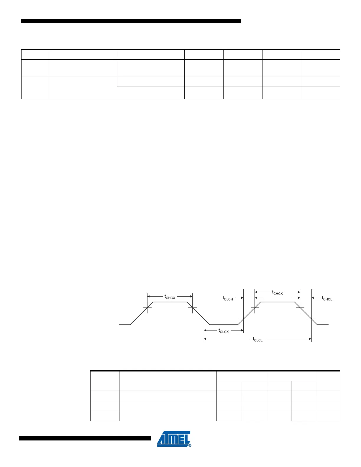
26.3 External Clock Drive Characteristics
Figure 26-1. External Clock Drive Waveforms
I
ACLK
Analog Comparator
Input Leakage Current
V
CC
= 5V
V
in
= V
CC
/2
– 50 50 nA
t
ACID
Analog Comparator
Propagation Delay
Common Mode Vcc/2
V
CC
= 2.7V 170 ns
V
CC
= 5.0V 180 ns
T
A
= -40°C to +85°C, V
CC
= 2.7V to 5.5V (unless otherwise noted) (Continued)
Symbol Parameter Condition Min. Typ. Max. Units
Table 26-1. External Clock Drive
Symbol Parameter
V
CC
= 2.7 - 5.5V V
CC
= 4.5 - 5.5V
Units
Min. Max. Min. Max.
1/t
CLCL
Oscillator Frequency 0 8 0 16 MHz
t
CLCL
Clock Period 125 62.5 ns
t
CHCX
High Time 50 25 ns

 Loading...


