53
AT90S2313
0839G–08/01
The Port B Input Pins address (PINB) is not a register; this address enables access to
the physical value on each Port B pin. When reading PORTB, the Port B Data Latch is
read, and when reading PINB, the logical values present on the pins are read.
Port B as General Digital I/O All eight pins in Port B have equal functionality when used as digital I/O pins.
PBn, general I/O pin: The DDBn bit in the DDRB register selects the direction of this pin.
If DDBn is set (one), PBn is configured as an output pin. If DDBn is cleared (zero), PBn
is configured as an input pin. If PORTBn is set (one) when the pin is configured as an
input pin, the MOS pull-up resistor is activated. To switch the pull-up resistor off, the
PORTBn has to be cleared (zero) or the pin has to be configured as an output pin The
Port B pins are tri-stated when a reset condition becomes active, even if the clock is not
active.
Note: n: 7,6…0, pin number.
Alternate Functions of Port B The alternate pin functions of Port B are:
• SCK – Port B, Bit 7
SCK, Clock input pin for memory up/downloading.
• MISO – Port B, Bit 6
MISO, Data output pin for memory uploading.
• MOSI – Port B, Bit 5
MOSI, Data input pin for memory downloading.
• OC1 – Port B, Bit 3
OC1, Output Compare Match Output. The PB3 pin can serve as an external output for
timer 1 compare match. The PB3 pin has to be configured as an output (DDB3 is set
[one]) to serve this function. See the timer description for further details, and how to
enable the output.
• AIN1 – Port B, Bit 1
AIN1, Analog Comparator Negative Input. When configured as an input (DDB1 is
cleared [zero]) and with the internal MOS pull-up resistor switched off (PB1 is cleared
[zero]), this pin also serves as the negative input of the on-chip Analog Comparator.
• AIN0 – Port B, Bit 0
AIN0, Analog Comparator Positive Input. When configured as an input (DDB0 is cleared
[zero]) and with the internal MOS pull-up resistor switched off (PB0 is cleared [zero]),
this pin also serves as the positive input of the on-chip Analog Comparator.
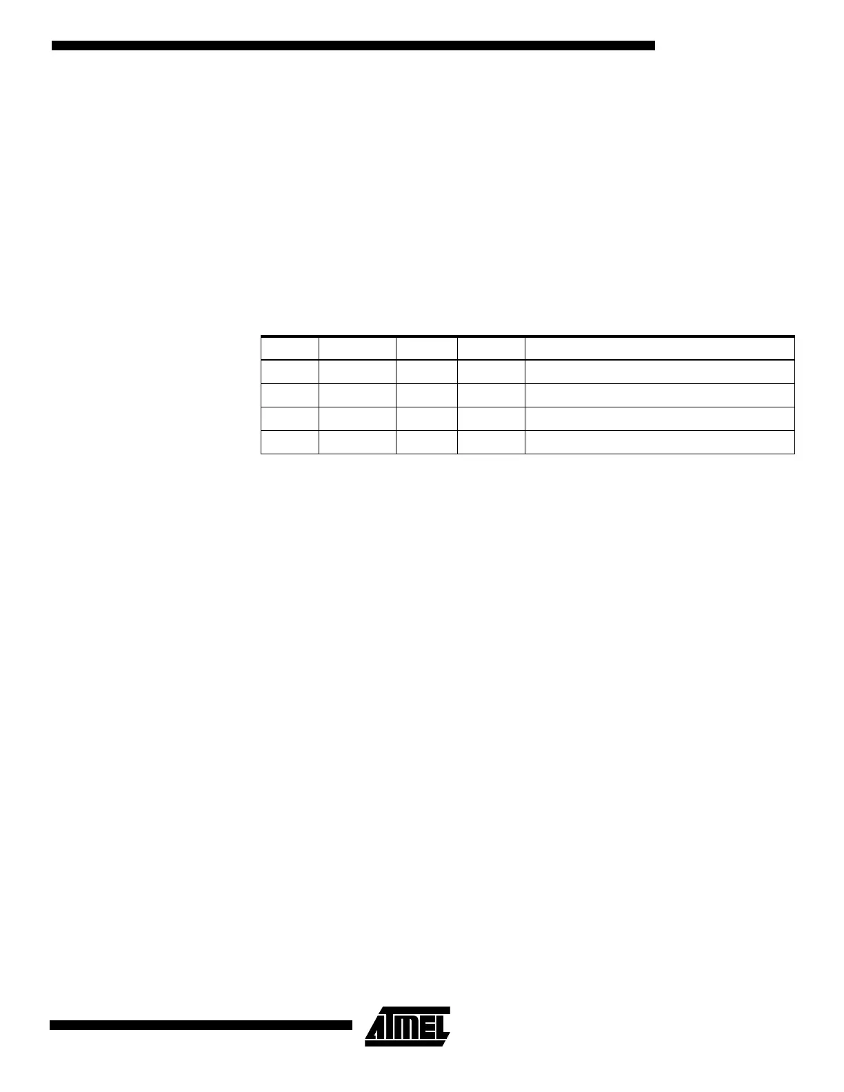
Table 18. DDBn Effects on Port B Pins
DDBn PORTBn I/O Pull-up Comment
0 0 Input No Tri-state (High-Z)
0 1 Input Yes PBn will source current if ext. pulled low
1 0 Output No Push-pull Zero Output
1 1 Output No Push-pull One Output

 Loading...


