C22
104
R27 51
C23105
PGND
C27
104
PGND
PGND
C28104
C29104
R34 1.5
R361.5
C32333
C33333
PGND
PGND
PGND
L4 10uH
L1 10uH
VCC28A
+28.5V
C36
1000u/35V
PGND
C38
102
C40
103
R40
3.3
R2410
C24104
PGND
C43
0.47u
C90
0.47u
C44
103
C93
103
R52
1
R93
1
PGND
C25
105
PGND
R25 10
R311
R321
R45
5.1K
R90
5.1K
PGND
R38
4.7K
R39
DNS
+28.5V
R44
4.7K
R47
DNS
+28.5V
PGND
SD
VALID
PWM_SR+
PWM_SL+
PWM_SL-
VALID
SD
PWM_SL+
PWM_SL-
PWM_SR+
PWM_SR-
SL-
SR-
GND
1
GND
2
GREG
3
/OTW
4
/SD_CD
5
/SD_AB
6
PWM_DP
7
PWM_DM
8
/RESET_CD
9
PWM_CM
10
PWM_CP
11
DREG_RTN
12
M3
13
M2
14
M1
15
DREG
16
PVDD_B
41
BST_B
42
BST_C
43
PVDD_C
44
PVDD_C
45
OUT_C
46
OUT_C
47
GND
48
GND
49
OUT_D
50
OUT_D
51
PVDD_D
52
PVDD_D
53
BST_D
54
GVDD
55
GND
56
PWM_BP
17
PWM_BM
18
/RESET_AB
19
PWM_AM
20
PWM_AP
21
GND
22
DGND
23
GND
24
DVDD
25
GREG
26
GND
27
GND
28
GND
29
GVDD
30
BST_A
31
PVDD_A
32
PVDD_A
33
OUT_A
34
OUT_A
35
GND
36
GND
37
OUT_B
38
OUT_B
39
PVDD_B
40
N13
TAS5112DFD
5
6
XC100C
WP12
7
8
XC100D
WP12
SROUT
SLOUT
PWM_SR-
PGND
C120104
C121104
R1341.5
R1361.5
C129333
C130333
PGND
PGND
PGND
PGND
VCC28A
R1321
R1311
C139
0.47u
C140
0.1u
C141
0.1u
C143
103
C142
103
R144
1
R145
1
PGND
L9 10uH
L1010uH
+28.5V
C133
1000u/35V
PGND
C135
102
C137
103
R140
3.3
R142
10K
R143
10K
SW+
SW-
9
10
XC100E
WP12
C26
104
PWM_SW-
PWM_SW+
PWM_SW+
PWM_SW-
R2080R
R2090R
R2100R
R2110R
R2120R
R2130R
PGND PGND
C66
103
C71
103
C65
103
C64
103
C9
104
C10
104
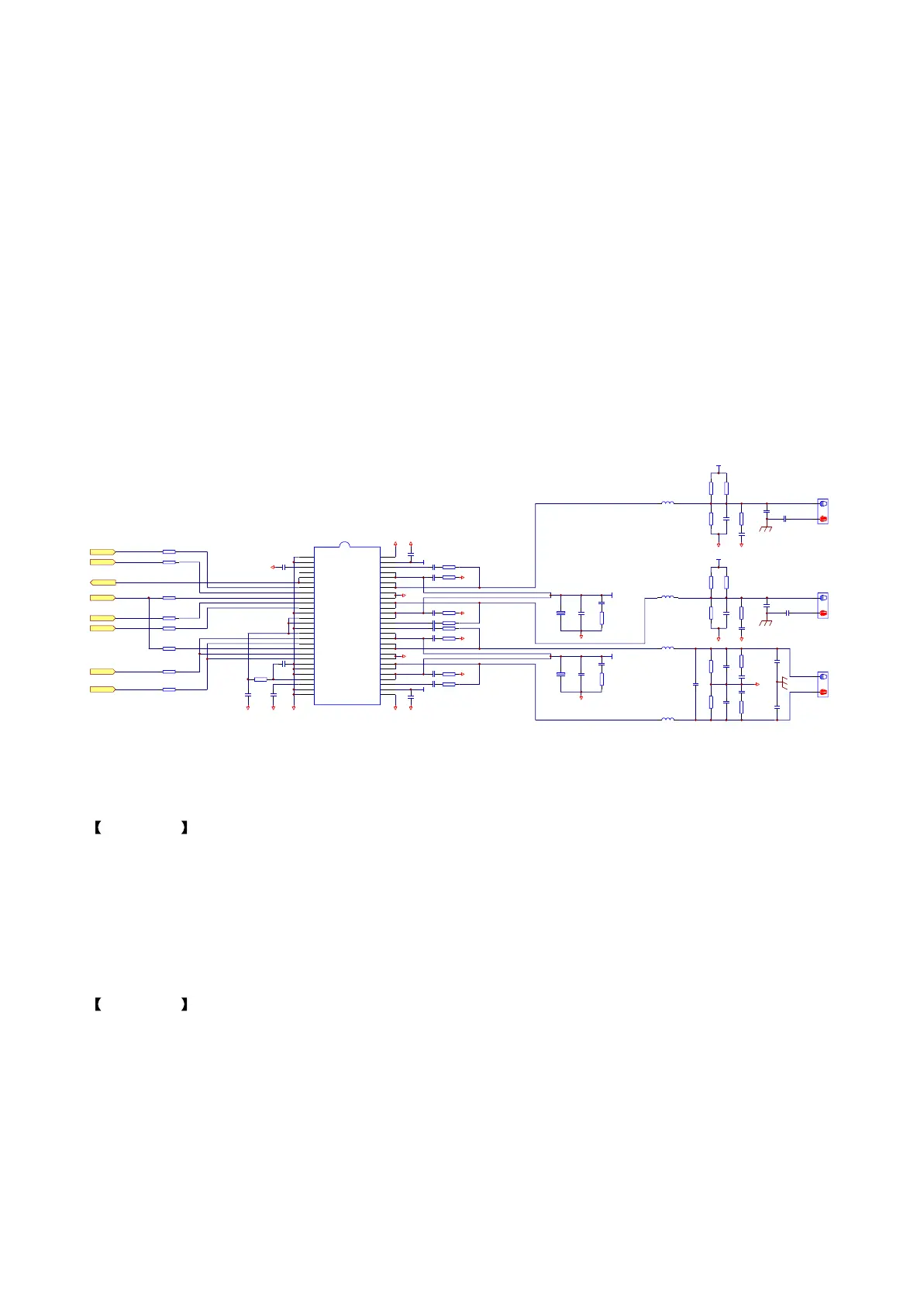
Figure 3.3.1.2 Power amplifying circuit diagram
Step 5: use DC level of multimeter to test voltage on output terminal, and find that voltage of SW+
and SW- is 6.09V, voltage of all other output is 14.02V and they are both +14V in normal conditions, so
we can judge that the capacitor of circuit between N13 (TAS5112) and output part has electric leakage,
change C139, C140, C141, C142, C143, C66, C71, but trouble is still not removed.
Step 6: after removing resistor R142, R143, voltage output of SW+ and SW- is +14V, which is
normal. We judge that one of R142 and R143 has trouble, after changing it, voltage of SW+ and SW-
changes to +6.02V, and trouble is still not removed.
Step 7: after changing N13 (TAS5112) directly, trouble is removed.
Conclusion: N13 is damaged inside, after connecting R142, R143, it will form loop with ground,
which will lead to abnormal working of N13 to make SD signal of pin 6 output low level, this signal
controls TAS5508 and performs self-protection function and cannot output signal, which makes us
consider that TAS5508 is damaged.
Example 6 MIC has no sound
Analysis and troubleshooting: when playing discs, use remote controller to open MIC item and there
is still no sound. Check power supply of 4558, CD4052, CS5340 and they are all normal. Use
oscillograph to test pin 6 input of 4558 and it is normal, pin 7 has no input, check R4, C6 and they are
both normal, so it is doubted that 4558 is damaged, after changing 4558, MIC is normal.
Example 7 Power amplifier has no sound
Analysis and troubleshooting: use multimeter to test power supply on power amplifier board XP503
and it is +29.6V, which is normal, Test power supply on XP101 and it is also normal, test HDET signal on
pin 24 of XS207 on power amplifier board and it is 0V; when working normally, if headphone is not
inserted, voltage on HDET should be about +3.3V. Test HDET signal on pin 7 of XS201 on power
amplifier board and it is 0V, which is abnormal, in normal conditions, if headphone is not inserted,
voltage in this place should be +2.9V; when power off and headphone is not inserted, use multimeter to
- 32 -