22
ENG
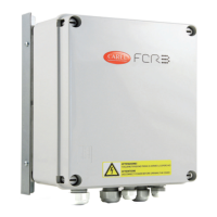
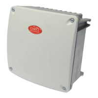
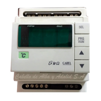
“FCR3 three-phase controller” +030222150 - rel. 1.3 - 12.01.2021
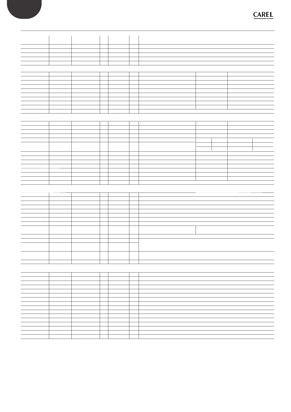
7.1 Summary table of operating parameters
name Modbus var range def. User setting
res.
UOM
description
MAC SID Fixed R 1 Type of unit = 311
REL SID 0 .. 255 R 1 Firmware release
HW SID 0 .. 255 R 1 HW release
TV SID 23/40 R 1 Voltage/10 40=400 , 23=230
TI SID 06/09/12/20/40 R 1 Current 06=6 A, 09=9 A, 12=12 A , 20=20 A, 40= 40 A
COILS
WE 1 0/1 0 1 Enable EOVR use 0=disabled 1=enabled
HZMEM 2 0/1 0 1 position of dipswitch 4 - S2 MEM 1=On (60Hz) 0=O (50Hz)
LINMEM 3 0/1 0 1 position of dipswitch 5- S2 MEM 1=On (QUAD) 0=O (LIN)
MINCUTMEM 4 0/1 1 1 position of dipswitch 6- S2 MEM 1=On (CUTOFF) 0=O (MIN)
FDEF 7 0/1 0 1 Reset default values 0= no action 1=enabled (one time)
SAVE 8 0/1 0 1 Save to memory (time) 0= no action 1=enabled (one time)
IOVR 9 0/1 0 1 Override Input 0=disabled 1=enabled
MODID 10 0/1 0 1 Digital input logic 0=norm. closed 1=norm. open
EOVR 11 0/1 0 1 Override output (only if WE=1) 0=disabled 1=enabled
CO12-16 12-16 0/1 0 1 Future uses
DISCRETE INPUTS
SEL 1 0/1 R 1 position of dipswitch 1- S2 1=On (MEM) 0=O (MAN) from FCR panel
HZFCR 2 0/1 R 1 position of dipswitch 4- S2 1=On (60Hz) 0=O (50Hz)
LINFCR 3 0/1 R 1 position of dipswitch 5- S2 1=On (QUAD) 0=O (LIN)
MINCUTFCR 4 0/1 R 1 position of dipswitch 6- S2 1=On (CUTOFF) 0=O (MIN)
BAUD1FCR 5 0/1 R 1 position of dipswitch 7- S2
9600 19200 34800
S2.7 OFF (ON) OFF
S2.8 OFF (OFF) ON
BAUD2FCR 6 0/1 R 1 position of dipswitch 8- S2
ALRTMP 7 0/1 R 1 Temperature alarm status 0=inactive 1=active
ALRPRC 8 0/1 R 1 Probe CC alarm status 0=inactive 1=active
ALRPRO 9 0/1 R 1 Probe open alarm status 0=inactive 1=active
STID 10 0/1 R 1 Digital input state SW1+SW2 0=open 1=closed
ALRM 11 0/1 R 1 Digital Input alarm status 0=inactive 1=active
ERRMEM 12 0/1 R 1 Memory error alarm 0=inactive 1=active
FCRON 13 0/1 R 1 FCR status 0= spento 1= acceso
DI15-16 14-16 0/1 R 1 Future uses
HOLDING REGISTERS
SADRMEM 1 1..255 1 1 Serial address device in saved to be used if all Dip S1 OFF
DELAYMEM 2 0 .. 100 100 1% DELAY value in memory
MAXMEM 3 50 .. 100 100 1% Memory value for maximum output 50-100 => Outmax 50%-100%
MINMEM 4 0 .. 40 40 1% Memory value for minimum output 0-40 => Outmin 0-40%
TEMPALM+ 5 -30- 105 85 1 Maximum temperature threshols for alarm (>= 101 the alarm is not activated)
TEMPALM- 6 -30- 105 -20 1 Minimum temperature threshols for alarm (<=-21 the alarm is not activated)
INMEM 7 0..100 0 1% Input value if override input is enabled (IOVR=1)
DELAYINMEM 8 0..100 100 1% Input DELAY value INMEM (high as default so as to start with delay if override)
ALMO 9 0..2 0 1
Output in the event of alarms and/or
o ine if serial control
0=0% - 1=50% - 2=100%
OUTMEM 10 0- 0% 1% Output value in memory for override
TIMEOUTL 11 15..256 30 1 Timeout on 485 (after this time, the blue LED goes o and the ALMO output is activated if
set by INMEM (then if IOVR==1), otherwise no action
TIMEOUT=TIMEOUTH*256+TIMEOUTL
TIMEOUTH 12 0-5 0 1
TIMESAVE 13 0.256 5 1
Saving timeout (minutes). After a time equal to TIMESAVE the parameters are checked; if
they have been changed, they are saved using function CO.8 (SAVE)
HR14-16 14-16 Future uses 0 1 Future uses
INPUT REGISTERS
SADRFCR 1 0 .. 255 R 1 Serial address set by Dip S1
DELAYFCR 2 0 .. 100 R 1 DELAY trimmer reading
MAXFCR 3 50 .. 100 R 1 Maximum trimmer reading 50-100 => Outmax 50%-100%
MINFCR 4 0 .. 40 R 1 Minimum trimmer reading 0-40 => Outmin 0-40%
TEMPER 5 -20 –100 R 1 Board internal temperature value (integer with sign)
INFCR 6 0.100 R 1 Analogue input voltage reading (0-100). The value depends on the setting of S2 (DIP3/DIP4)
OUTMIN 7 0 .. 40% R 1% Minimum output set
OUTMAX 8 50%-100% R 1% Maximum output set
OUTFCR 9 0%-100% R 1% Output current
IN 10 0-100 R 1 Current value of IN after DELAY
OUTREAL 11 0-100 R 0 Real Output
MAC 12 311 R 0 MAC
REL 13 0 to 255 R 0 Firmware Release
HW 14 0 to 255 R 0 HW Release
TV 15 23/40 R 0 Voltage /10
TI 16 6/9/12/20/40 R 0 Current
Tab. 7.a