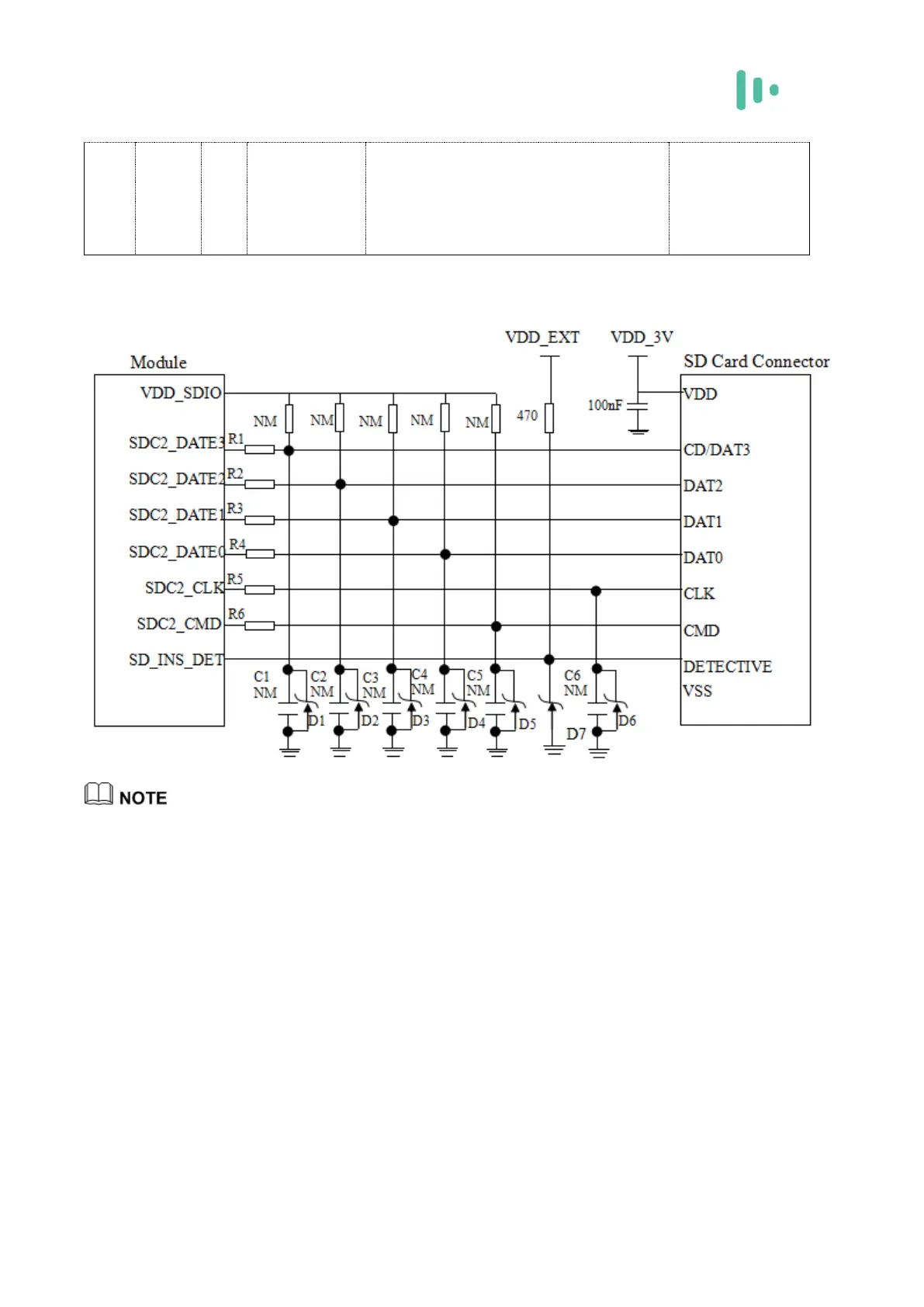
The SD card reference design for the C100QM/C10QM module is shown below:
Figure 3-23 SD card interface reference circuit diagram
✧ SD card circuit routing considerations:
✧ The SD card power supply is 3V with a voltage range of 2.7~3.6V, which needs to be
externally supplied and has a minimum current of 800mA.
✧ The maximum output current of the module output power supply VDD_SDIO is
50mA, which can only be used for SDIO bus pull-up;
✧ The SD card has a clock frequency of up to 200 MHz, and the trace is best controlled
by 50 ohms.
✧ The length of the signal line should be less than 25mm, and the spacing of the signal
line should be 2 times the line width and cover the ground and keep away from other