NVF5 Series User Manual Chapter 3 Installation and Wiring
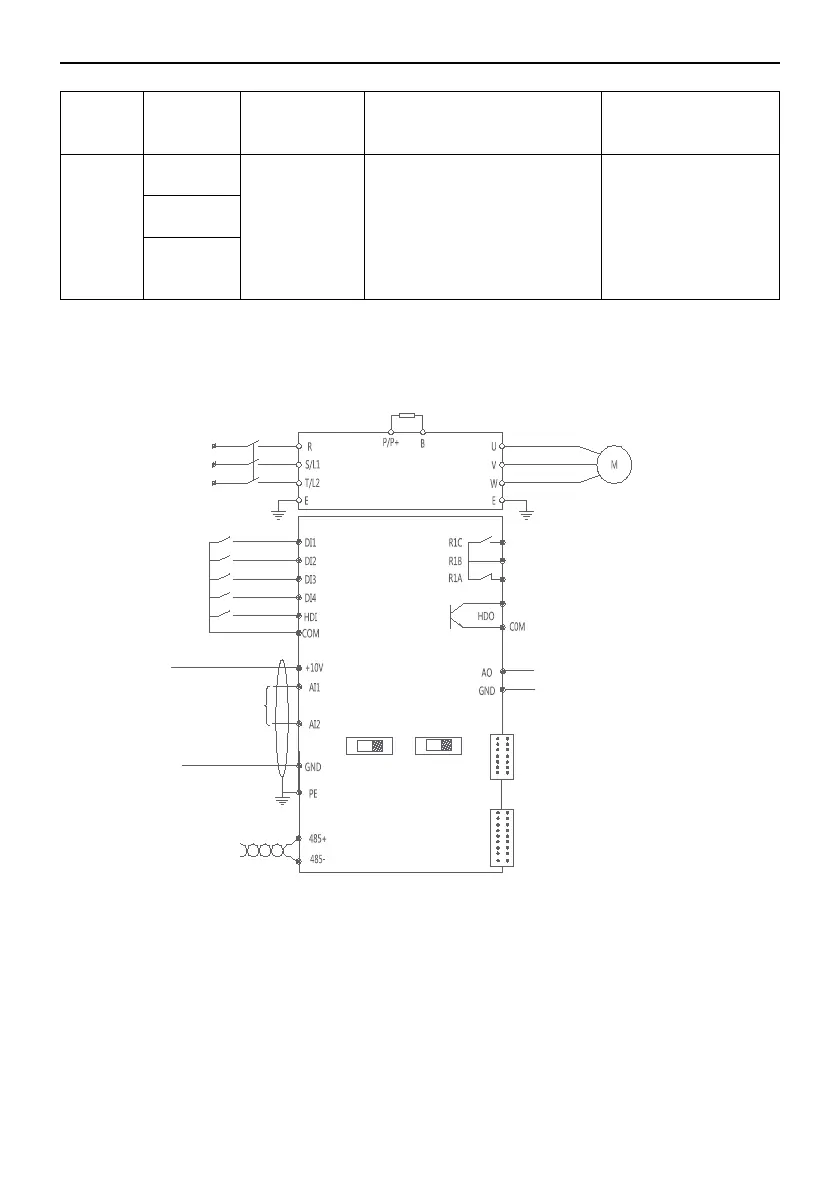
3.5.3 Power terminal and I/O terminal block diagram
V:(-10~10)V
I:(0~20)mA or (4~20)mA
RS485 communication
Brake resistor
Main circuit terminal
Control circuit terminal
QF
Power grounding
Motor grounding
A11
V1I1
2 x Analog input
Analog input power supply
Analog input common
AO
Programmable
Multifunction
AOVAOI
Single-phase input power
230V 50/60Hz
Three-phase input power
380V~440V 50/60Hz
V:(0~10)V
I:(0~20)mA or (4~20)mA
Analog output
Output
J2、J3 Multifunction extension card interface
J2 Multifunction interface
J3 Multifunction interface
Programmable relay outputs
Programmable open collector
Input
high-speed output
Figure 3-5-3 Inverter Terminal Wiring Diagram
AO Dip Switch:Left,(0~20)mA or (4~20)mA Analog Current Ouput;Right,( 0~10)
V Analog Voltage Output.
AI1 Dip Swith:Left,( 0~20)mA or (4~20)mA Analog Current input;Right,( 0~10)
VAnalog Voltage input.
AI2:Current Output need to be customized
COM
Supply
+
24V Common
between COM and
Relay
Output
R1A
Relay
Output
Programmable Relay
Output Terminals,refer to
parameter F6.02
R1A-R1B
:
N.C.
;
R1B-R1C
:
N.O.
Contact Capacity
:
NO 5A /NC 3A
250V
(
AC
)
R1B
R1C
- 21 -