Technical description
4-28 HF SSB Transceiver 9323/9360/9390/9780 Technical Service Manual
The temperature compensating components IC8/A, D8 and D9 ensure that the set
viewing angle remains constant over the operating temperature range. To enable
the output of IC8 to be negative with respect to reference ground, it is connected
to the +5 V and the −7 V supplies.
A second temperature sensor R53 monitors the temperature and reduces the back
light by switching off V13 at 60°C followed by V6 at 65°C. The back light returns
to its normal setting for a period of two minutes when any control function is
initiated.
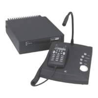
Microphone keypad
The microphone assembly incorporates a microphone, a PTT button, a keypad and
an encoder.
The keypad can be used to control most of the transceiver’s functions. It consists
of a panel overlay forming a 3 × 4 matrix. The three columns and four rows are
connected to encoder IC1 [104-02975]. When each button is pressed, it outputs
serial data from IC1 pin 1. This is fed to the control head via J1 pin 4. From here,
it is passed via a buffer/inverter IC7/A to the RXD input of the microprocessor
IC2 pin 24. The microprocessor reads the data and performs the appropriate
function for the particular button that was pressed.
The encoder IC1 receives its 5 V supply from the "A" rail via shunt zener diode
V1 through series resistor R1.
The back lighting to the buttons is provided by four LEDs, which are connected
via two 470 Ω current limiting resistors to the "A" rail.
Data input/output
The connector J3 on the front of the control panel provides input from the
microphone assembly (see page 4-28, Microphone keypad). It also has a secondary
function when connected to a computer with XP software. It provides an
input/output data facility for channel programming and set up.
When set up in Program mode, data from the computer is applied to J3 pin 4. This
is the same data input path used by the microphone and follows the same path to
the RXD input of the microprocessor IC2 pin 4. The data from the microprocessor
IC2 pin 25 (TxD line) is passed to the buffer/inverter V7. From here the data goes
via P3 pin 3 to J3 pin 5 and then to the computer input.