Technical description
HF SSB Transceiver 9323/9360/9390/9780 Technical Service Manual 4-35
Selective calling
The selective calling facility is fitted as standard in the transceiver (it is optional
for the 9390). To use it, it must be enabled.
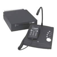
A call is initiated by pressing the Call button on the microphone, or F1 on the
front control panel. On recognising the request for a call, the microprocessor
IC101 on the Microprocessor and Audio PCB [1 04-02976 Sheet 1] checks that
the channel selected has selcall enabled. If it is enabled, the microprocessor
generates the required data for the selective call from the Call Address and Self
Ident code configured in the transceiver.
The microprocessor IC101 [1 04-02976 Sheet 1] sets the dividers in the tone
generator IC106 to produce the correct FSK tones before applying the generated
data. The resulting FSK tones from IC106 pin 17 are filtered by R135/A, C120,
R136 and C117. This is applied via R213 and C215 to the input of the combining
amplifier IC204/A (see Sheet 2). The transistor V204 is switched off. This
removes the short circuit during transmission and enables the FSK tones to be
applied to the combining amplifier IC204/A. The FSK tones are also attenuated by
R131 and R132 (see Sheet 1) and are applied as side tone to the input of the
speaker audio amplifier IC306 (beeps input). At the same time, the microprocessor
IC101 generates a PTT command so that the FSK tones are transmitted. On
completion of the coded transmission, the PTT signal is removed and the
transceiver returns to the Receive mode.
In Receive mode, the FSK audio appears at the output of the audio preamplifier
IC204/A on the Rx/Exciter PCB [1 04-02972 and 04-03135 Sheet 2]. The audio
is passed by ribbon cable from P201 pin 9 to P102 pin 9 on the Microprocessor
and Audio PCB [1 04-02976 Sheet 2]. It is then applied via C206, C302 and
R302 to the input of the dual BPF IC301/A and IC301/B (see Sheet 3). The audio
from the filter output (pin 7) is fed to the input of the FSK decoder IC302 pin 2.
The voltage controlled oscillator (part of IC302) is automatically calibrated on
power up (see page 4-34, Calibration). In the absence of FSK signals, the lock
detect output from pin 6 will fluctuate and the resulting charge on C312 will be
less than half the supply voltage. The voltage is applied via R312 to the
comparator input (pin 8) resulting in a low output from pin 7. Some of the output
is fed back via R313 to the input to provide hysteresis. The comparator output is
taken via D303 to the non-inverting input of IC303/B. This results in a low output
from IC303/B, which effectively cuts off V302. When the FSK signals are
detected, the lock detect output goes high. The resulting high comparator output
reverse biases D303, thus enabling IC303/B.
When FSK signals are received, data appears on the phase detector output
(pin 11). This is applied to the data filter IC303/A and associated components.
This is an LPF at approximately 80 Hz, which passes the resulting data to the
input of IC303/B. The data filter output is also peak rectified by D301, D302,
C320 and C321. The voltages on the two capacitors are summed at the inverting
input of IC303/B to give a reference voltage equal to the main frequency of the
FSK signal. The result is that IC303/B regenerates the data and ignores any
frequency shift in the RF path.