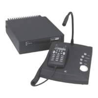
Technical description
HF SSB Transceiver 9323/9360/9390/9780 Technical Service Manual 4-29
"S"+ RF indicator
An approximate indication of the receive signal strength and transmit output
power is displayed in the form of a bar graph on the LCD. These two signals are
derived from the AGC in receive and the forward power detector in transmit.
The AGC voltage from the RX/Exciter PCB enters the Microprocessor and Audio
PCB at P102 pin 5 [1 04-02976 Sheet 1]. This is connected via D101 and R101
to the load resistor R104.
The forward power detector is derived from the PA assembly and enters the
Microprocessor and Audio PCB at P101 pin 10. It is then connected via R102,
D102 and R103 to the load resistor R104.
The receive signal strength and the transmit output power signals do not appear at
the same time. Therefore they can share the same path and are OR gated across
R104 ("S" + RF). The signals are available from P201 pin 4 [104-02976] via a
coupling cable to the front panel P4 pin 4 [104-02974] and to the Remote
Control connector P204 pin 8 [104-02976] for the control head. The signals are
then passed through an RF filter (R43 and C37) to microprocessor IC2 pin 1.
The microprocessor IC2 measures the analogue level of the AGC in receive and
the forward power detector in transmit [104-02974]. The resulting digital
information is passed to the LCD display H1. The microprocessor in the LCD
assembly translates the information to produce the appropriate signal levels on the
bar graph.
In receive, the analogue level of the AGC is measured by IC2. The minimum
signal commences at 4.5 V and falls to 0.25 V for maximum signal strength. In
transmit the measurement is reversed—it begins at 0 V for a zero output and rises
to 4.25 V for maximum output power.
Mute indicators
The S’Call Mute and Voice Mute buttons incorporate LED indicators and are lit
when one of the mute functions is selected. These are controlled by the
microprocessor IC2 setting the appropriate output port of IC1 pin 11 or 12 high,
via the I
2
C bus. This causes either V4 or V5 to conduct and to light the respective
LED.
Front panel back light
The front panel back lights help locate the buttons and control knobs for night-
time operation. The panel consists of 16 LEDs divided into four groups. They are
connected between the "A" rail and transistor switch V11 to ground. Each group
of four LEDs has its own 390 Ω current limiting resistor. When the back lighting
to the LCD is set to minimum, transistor V11 is switched off reducing the
intensity of the front panel back light.