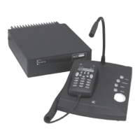
Technical description
HF SSB Transceiver 9323/9360/9390/9780 Technical Service Manual 4-33
For low power, the sum of the lower section of the divider chain uses the same
components as used for high power, as well as V7 off (i.e. gate at 0 V), resistors
R17 (SOT) and R18. The resistor R17 is selected for low power when the power is
<12 W PEP.
The output of the forward detector D1 is also applied to V9 via an averaging
detector circuit consisting of R23 and C83. When the average of the signal
exceeds the peak detector circuit (this occurs when in Tune mode, CW (morse)
and in some data transmissions), V9 takes control and reduces the output power.
The output of the reflected rectifier D2 is applied via resistor divider R26 and R25
to the input of V10. The rectifier D2 takes control of the ALC when the reflected
power exceeds 10 W (> 2:1 VSWR).
The peak output collector swing is monitored by R70 and D10 for V24, and R73
and D11 for V23. The diode cathodes are ORed and applied via resistor divider
R71 and R72 to V11. The transistor V11 will conduct and limit the collector peak
to 42 V to prevent damage to the output transistors.
The battery voltage is monitored by V6. When the supply voltage ("A" rail) drops
to about 12 V, the voltage at the base of V6 (set by the resistor divider R11 and
R12) will fall to 4.3 V and cause V6 to conduct. This will start to raise the voltage
across R19 (part of the forward detector resistor chain) and change the threshold
of the forward ALC detector. The ALC detector will start to reduce the output
power and, as the control is linear, a further reduction in supply voltage will
continue to lower the output power.
If the heatsink exceeds 80°C, PTC resistor R34 rapidly increases in value,
reducing the reference ALC threshold level to the comparator IC3/B. This lowers
the output power and prevents the heatsink from exceeding 90°C.
The protection circuit consists of IC3/A and associated components. It
simultaneously monitors the output transistors, collector swing (applied to IC3/A
pin 3) and the forward detector output of D1 (applied via R27 to IC3/A pin 2). In
the event of a relay failure, which results in no signal at the antenna output, the
output of IC3/A (coupled via D9 into the ALC control circuit) will go high. This
will reduce the drive to the output transistors to a safe level by lowering the gain
of the input amplifier V14.