JHT01 Service Manual
4-10
3.10.2 Battery Connector
Pin 1: BATT+
Pin 2: BATT+
Pin 3: CNT1 (ID)
Pin 4: CNT2 (B/I)
Pin 5:
EC_SMCA (SMC)
Pin 6:
EC_SMDA (SMD)
Pin 7: TS_A (TS)
Pin 8: GND
Pin 9: GND
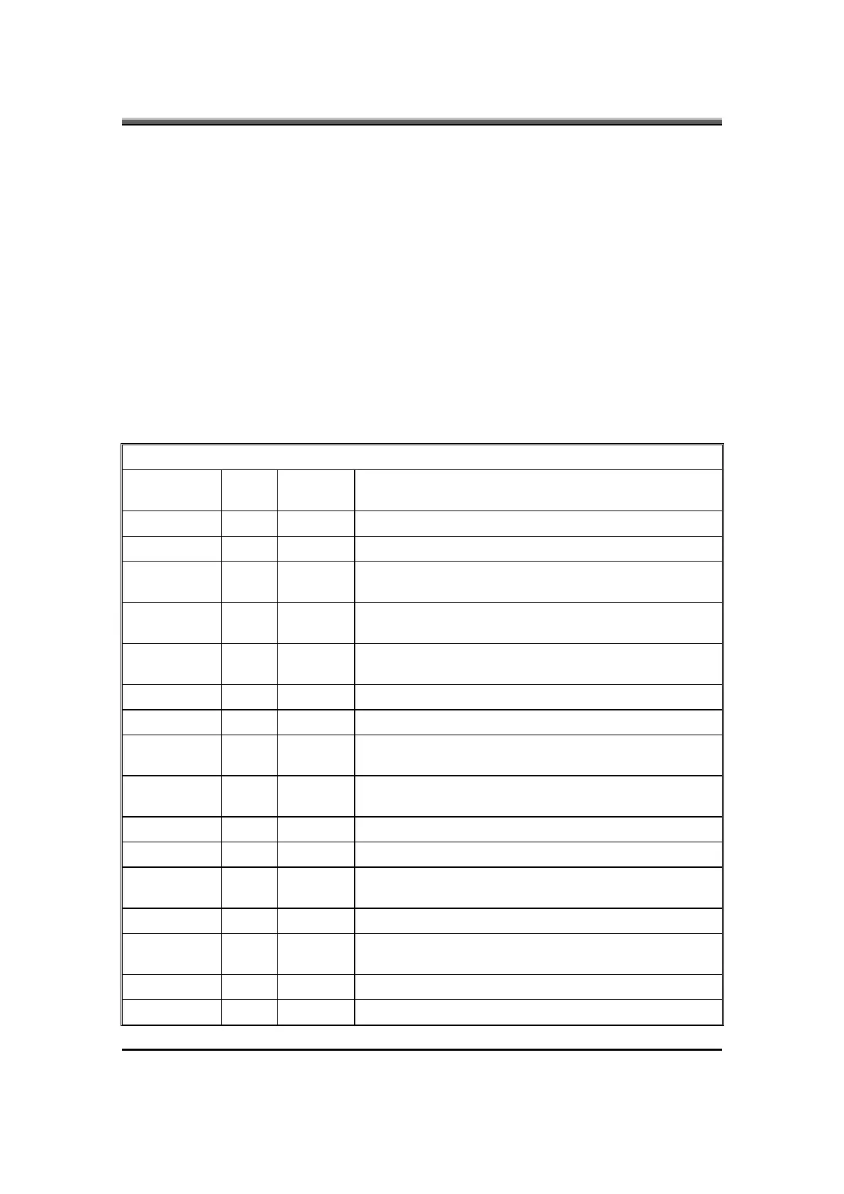
3.10.3 Interface between Power with M/B
DC/DC
Signals I/O Voltage
Level
Description
SUSP# I 0~3.3V Low Active, system suspend control signal
51ON# I 0~floating Low Active, POWER ON control signal.
FSTCHG I 0~3.3V
High Active, ENE926 use this pin to control the fast charge of
charge
ACOFF I 0~3.3V
High Active, turn off the Adaptor power for battery automatic
learning cycle
ACIN O 0~3.3V
High Active, provide to ENE926 to mean the Adaptor power is
present
VGATE O 0~3.3V High Active, it will go high when +CPU_CORE is ready
VR_ON I 0~3.3V High Active, turn on/off the +CPU_COREP & VID_VCC
BATT_TEMP
O 0~3.3V
Analog signal, ENE926 using this voltage level to calculate
battery’s temperature
IREF I 0~3.3V
Analog signal, ENE926 using this voltage for setting charge
current
VID [0..6] I 0~3.3V The +CPU_CORE voltage depends on those PIN’s VID [6..0]
CHGRTC O 3.3V Charge RTC-battery power source
EC_SMB_CK1,
EC_SMB_DA1
I/O 0~5V
Interface of Smbus, communicate between ENE926 and smart
battery
SYSON I 0~3.3V High Active, ENE926 use this pin to control the SYSON signal
BATT_AOVP O 0~3.3V
Analog signal, ENE926 using this voltage level for battery over
voltage protection
PSI# I 0~1.05V Analog signal, enable CPU_CORE regulator at light load mode.
DPRSLPVR I 0~1.05V Analog signal; control CPU C3, C4 signal.