2. Technical Description 9751 Installation Guide
Page 12 11976798
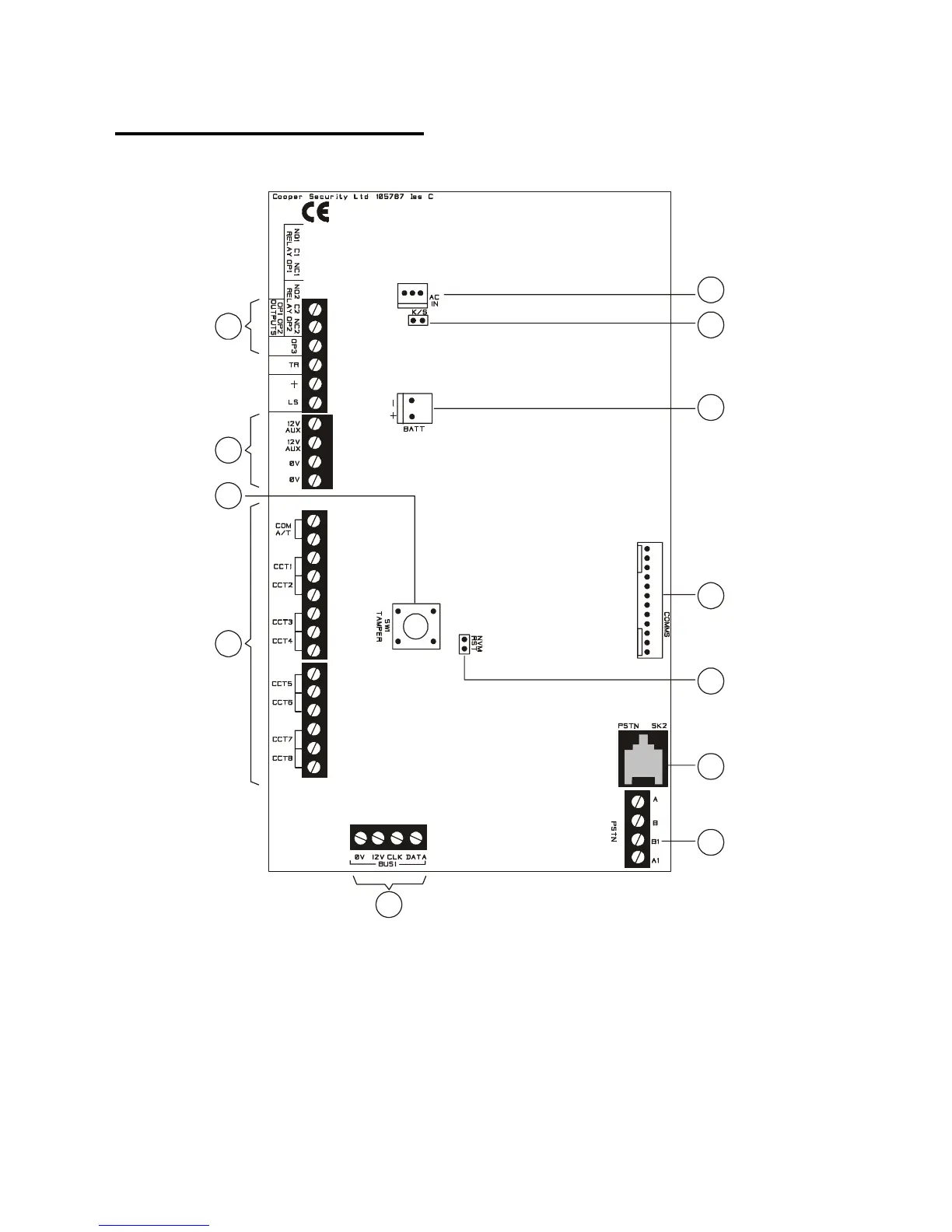
Control Unit PCB Layout
Figure 3 shows the layout of the PCB used in the control unit.
3
1
2
4
5
6
7
9
8
10
11
12
1. Outputs (3 open collector outputs) 8. NVM Reset pins
2. AUX power 9. Plug-by (standalone) communicator connector
3. Lid tamper switch 10. Battery connector
4. Zone connectors 11. Kick Start pins
5. Keypad and expander bus (bus 2 not fitted) 12. 21VAC from transformer
6. Telephone line terminals for built-in communicator
7. Telephone line socket for built-in communicator
Figure 3. Control Unit PCB Layout