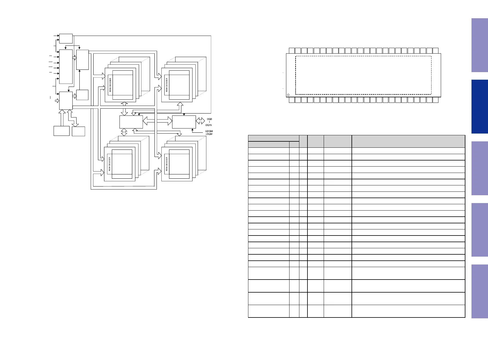
W9864G6KH-5 Block diagram
W9864G6KH
Publication Release Date: Nov. 12, 2013
- 6 - Revision A02
6. BLOCK DIAGRAM
CLK
CKE
A10
CLO CK
BUFF ER
COMMA ND
DECO DER
ADDRESS
BUFF ER
REFRESH
CO UNT ER
CO LUM N
CO UNT ER
CONTROL
SIGN AL
GENER ATOR
MO DE
REGI STER
COLUMN DECO DE R
SENSE AMPLIFIER
CELL ARRAY
BANK #2
COLUMN DECO DE R
SENSE AMPLIFIER
CELL ARRAY
BANK #0
COLUMN DECO DE R
SENSE AMPLIFIER
CELL ARRAY
BANK #3
DATA CONTRO L
CI RCUI T
DQ
BUFF ER
COLUMN DECO DE R
SENSE AMPLIFIER
CELL ARRAY
BANK #1
NOT E:
The cell array configuration is 4096 * 256 * 16
A0
A9
BS0
BS1
CS
RAS
CAS
WE
A11
PCM1690 (HDMI : U1048)
PCM1690 Pin Function
TERMINAL
I/O
PULL-
DOWN
5-V
TOLERANT
DESCRIPTION
NAME PIN
RSV2 1 — — — Reserved, tied to analog ground
RSV1 2 — — — Reserved, left open
RSV2 3 — — — Reserved, tied to analog ground
RSV1 4 — — — Reserved, left open
RSV2 5 — — — Reserved, tied to analog ground
LRCK 6 I Yes No Audio data word clock input
BCK 7 I Yes No Audio data bit clock input
DIN1 8 I No No Audio data input for DAC1 and DAC2
DIN2 9 I No No Audio data input for DAC3 and DAC4
DIN3 10 I No No Audio data input for DAC5 and DAC6
DIN4 11 I No No Audio data input for DAC7 and DAC8
VDD 12 — — — Digital power supply, +3.3 V
DGND 13 — — — Digital ground
SCKI 14 I No Yes System clock input
RST 15 I Yes Yes Reset and power-down control input with active low
ZERO1 16 O No No Zero detect ag output 1
ZERO2 17 O No No Zero detect ag output 2
AMUTEI 18 I No Yes Analog mute control input with active low
AMUTEO 19 O No Yes Analog mute status output(1) with active low
MD/SDA/DEMP 20 I/O No Yes
Input data for SPI, data for I2C(1), de-emphasis
control for hardware control mode
MC/SCL/FMT 21 I No Yes
Clock for SPI, clock for I2C, format select for hardware
control mode
MS/ADR0/RSV 22 I Yes Yes
Chip Select for SPI, address select 0 for I2C, reserve
(set low) for hardware control mode
TEST/ADR1/RSV 23 I/O No Ye s
Test (factory use, left open) for SPI, address select 1
for I2C, reserve (set low) for hardware control mode
1
2
3
4
5
6
7
8
9
10
11
12
13
14
15
16
17
18
19
20
21
22
23
24
48
47
46
45
44
43
42
41
40
39
38
37
36
35
34
33
32
31
30
29
28
27
26
25
RSV2
VCC2
AGND2
RSV2
VOUT1
VOUT2
VOUT3
VOUT4
VOUT5
VOUT6
VOUT7
VOUT8
RSV2
AGND1
VCOM
VCC1
RSV2
RSV1
RSV2
RSV1
RSV2
LRCK
BCK
DIN1
DIN2
DIN3
DIN4
VDD
DGND
SCKI
RST
ZERO1
ZERO2
AMUTEI
AMUTEO
MD/SDA/DEMP
MC/SCL/FMT
MS/ADR0/RSV
MODE
PCM1690
ThermalPad
PCM1690
SBAS448A–OCTOBER 2008 –REVISED JANUARY 2009..............................................................................................................................................
www.ti.com
DCA PACKAGE
HTSSOP-48 (12 mm x 8 mm)
(TOP VIEW)
TERMINAL FUNCTIONS
TERMINAL
PULL- 5-V
NAME PIN I/O DOWN TOLERANT DESCRIPTION
RSV2 1 — — — Reserved, tied to analog ground
RSV1 2 — — — Reserved, left open
RSV2 3 — — — Reserved, tied to analog ground
RSV1 4 — — — Reserved, left open
RSV2 5 — — — Reserved, tied to analog ground
LRCK 6 I Yes No Audio data word clock input
BCK 7 I Yes No Audio data bit clock input
DIN1 8 I No No Audio data input for DAC1 and DAC2
DIN2 9 I No No Audio data input for DAC3 and DAC4
DIN3 10 I No No Audio data input for DAC5 and DAC6
DIN4 11 I No No Audio data input for DAC7 and DAC8
6 Submit Documentation Feedback
Copyright © 2008–2009, Texas Instruments Incorporated
Product Folder Link(s): PCM1690
58
Caution in
servicing
Electrical Mechanical Repair Information Updating
 Loading...