Contents
4
Contents
About This Document........................................................................................................................................................7
Related Documentation..............................................................................................................................................7
Support Information...................................................................................................................................................7
Chapter 1: About the Digi Connect ME Family of Embedded Modules.............................................................................8
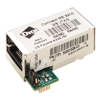
Digi Connect ME and Wi-ME Embedded Modules ..................................................................................................9
Types of Modules.....................................................................................................................................................10
Connectors: Power and Device Interface.................................................................................................................12
Connectors: Module JTAG Interface.......................................................................................................................14
Connectors: Ethernet Interface.................................................................................................................................16
JTAG Jumper..................................................................................................................................................17
Hard Reset ......................................................................................................................................................17
Connectors: Antenna................................................................................................................................................18
Module LEDs...........................................................................................................................................................19
Chapter 2: About the Development Board...........................................................................................................................20
Basic Description .....................................................................................................................................................21
Port Descriptions......................................................................................................................................................25
Primary Serial Port, P1...................................................................................................................................25
Secondary Serial Port, P2...............................................................................................................................26
RS232-Enable Pin Header, P5........................................................................................................................26
GPIO Port, P7.................................................................................................................................................27
Connectors and Blocks.............................................................................................................................................28
Embedded Module Connector, P10................................................................................................................28
Module JTAG Interface Connector, P11........................................................................................................31
JTAG Debugger Connector, P12....................................................................................................................33
Logic Analyzer Header, P3.............................................................................................................................34
Switches and Push Buttons ......................................................................................................................................35
GPIO Switch Bank 1, SW3 ............................................................................................................................35
User Push Button 1, SW1...............................................................................................................................35
User Push Button 2, SW2...............................................................................................................................35
Reset, SW4 .....................................................................................................................................................36
Power On/Off Switch, SW5 ...........................................................................................................................36
Development Board LEDs .......................................................................................................................................37
Power Jack P15 ........................................................................................................................................................39
Test Points................................................................................................................................................................40
 Loading...