E8 158004.B00
PIN SIGNAL
(AUDIO)
SIGNAL
(A/D)
VGA
PIN
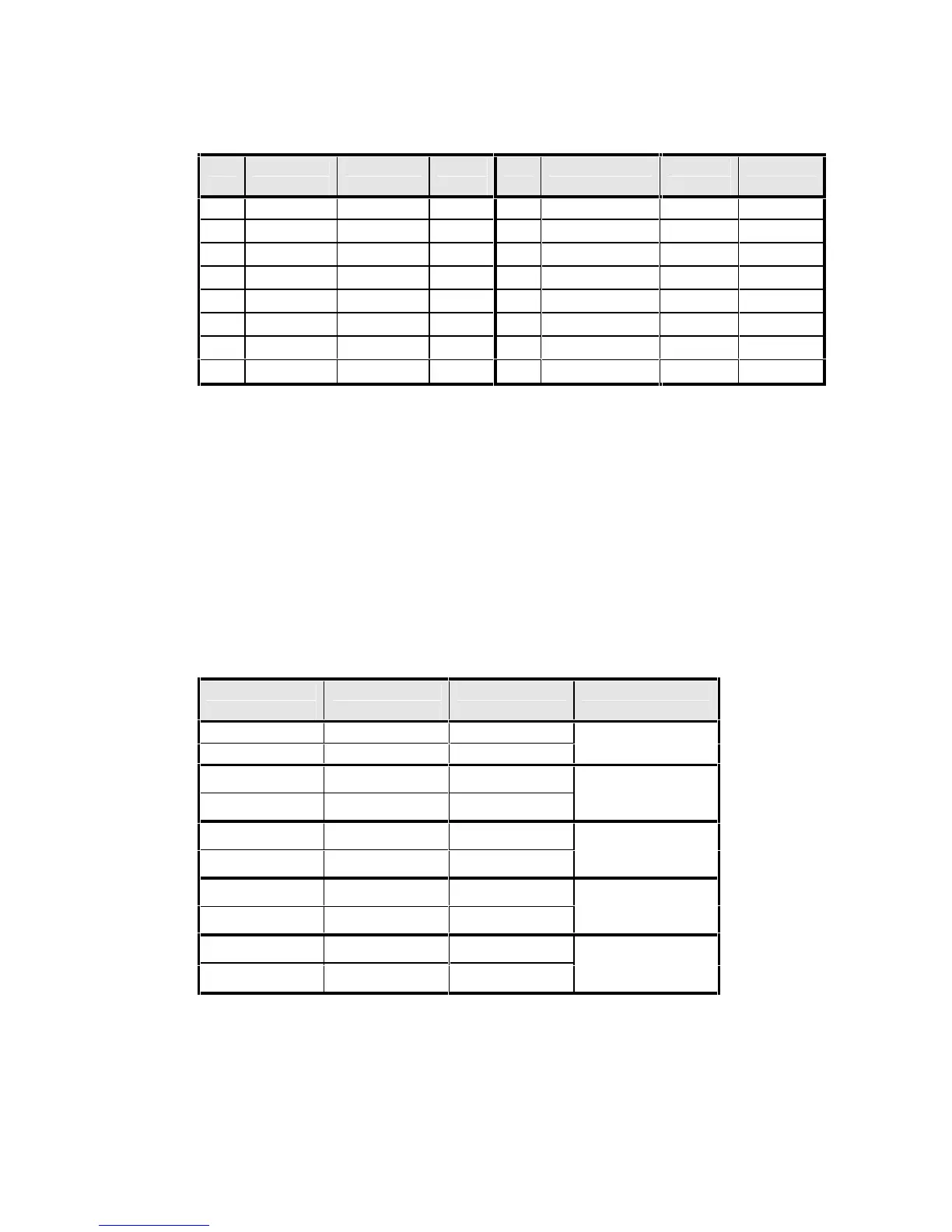
PIN SIGNAL
(AUDIO)
SIGNAL
(A/D)
VGA PIN
1 MIC IN VREF - 2 LINE_IN_R ADC0 -
3 ADCGND ADCGND - 4 LINE_IN_L ADC1 -
5 ADCGND ADCGND - 6 LINE_OUT_R ADC2 -
7 ADCGND ADCGND - 8 LINE_OUT_L ADC3 -
9 SUS_RES SUS_RES - 10 RED RED 1
11 GREEN GREEN 2 12 BLUE BLUE 3
13 AGND AGND 6, 7, 8 14 HSYNC HSYNC 13
15 VSYNC VSYNC 14 16 GND GND 5, 10
TABLE E9 - J6 VGA AND A/D CONNECTOR PIN ASSIGNMENTS
E.6 PanelLink CONNECTOR
Connector J7 is SIL header. It has eight pins on REV A TP400 boards, and ten pins
on the REV B boards. The connector is from the Hirose DF13 family.
The connector carries four twisted pair signals. The REV B board also has power
pins, suitable for powering an LCD so long as it is close by (it is unlikely that the
regulation of the power would be adequate at a distance of 10m).
J7 PIN (REV A
BOARD)
J7 PIN (REV B
BOARD)
SIGNAL DESCRIPTION
-
1 3.3V or 5V
-
2 GND
Power for LCD
1 3 TX2 +
2 4 TX2 -
TMDS signals:
Red data
3 5 TX1 +
4 6 TX1 -
TMDS signals:
Green data
5 7 TX0 +
6 8 TX0 -
TMDS signals:
Blue data
7 9 TXC +
8 10 TXC -
TMDS signals:
Clock
TABLE E10 - J7 PANEL LINK CONNECTOR PIN ASSIGNMENTS
Pin 1 of the J7 connector can be identified by looking at the silk-screen legend on the
TP400 PCB. A ’1’ symbol is placed close to pin 1.