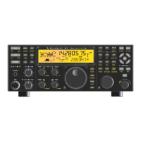
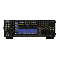
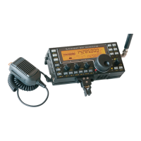
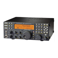
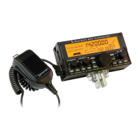
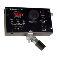
Theory Of Operation
Please referto the block diagram of the K3 shown at the end of this section. Schematics and additional details
can be found onthe Elecraft web site.
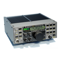
RF BOARD
The RF PCB (Printed Circuit Board) is the heart ofthe K3 transceiver, both physically and electrically. During
assembly, it servesas an attachment point for other PCBs as well as chassis panels, acting asthe glue that holds
things together. During operation, the RF board provides signal routing to and from all modules.
Over two-thirds of the RF board’s components are surface mount devices (SMDs), located on the bottom side of
the board. These are pre-installed andtested at the factory.The use of SMDs minimizes stray coupling in RF
circuits, reduces system cost, and allows the K3 to fit in a modest-size enclosure, compatible with home or field
operation.
The RF board is divided into several functional areas, which are described below.
Low-Pass Filters (LPFs)
The relay-switched low-pass filters, used during both transmit and receive, are located in the back-right corner
of the RF board. These filters can easily handle 100 watts, and are common to boththe K3/10 and K3/100.
Some LPFs cover one band, while others cover two bands that are close in frequency. The input tothe LPF
section comes from the KPA3 100-W amplifier module, if installed; if there’s no KPA3, the input comes from
the 10-W amplifier (see below). The output of the low-pass filters isrouted through the forward/reflectedpower
bridge, then on to either the antenna input module (KANT3), or the KAT3 automatic antennatuner, which plugs
in at far right.
Low-Power Amplifier (LPA) and T/R Switching
The large hole near the back-middle area of the RF PCB is where the 10-W low-power amplifier module plugs
in. The LPA hasthree connectorsthat mate with the RF board, and its power transistors attach to the rear bottom
cover, which serves as a heat sink.This construction method allows the 10-W module to be tested separately
during production. Also in this area is the T/R (transmit/receive) switch, but you’ll need to turn the RF board
upside down to see most of the components. The K3’s T/R switch uses high-power, high-isolation PIN diodes
ratherthan relays, resulting in no switching noise during keying.
Low Power Amplifier (LPA)
The low-power amplifier module is capable of up to 12 W power output, and in the case of the K3/10, isthe
final amplifier stage. In the K3/100, it provides drive to the KPA3 module. The LPA has three gain stages, the
last two of which use high-power MOSFET transistorsto allow coverage up through 6 meters. At the input to
the first gain stage is a 5-dB attenuator, which is switched in under firmware control at certain power levelsto
optimize transmit gain distribution.
Band-Pass Filters (BPFs)
At back-left isthe bank of ham-band BPFs. These filters are just wide enough to cover each ham band, so they
provide good rejection of IMD products during both transmit and receive. Hi-Q components, including large
toroids, ensure low loss and high signal-handling capability. General coverage receive capability can be added
tothe K3 with the KBPF3 option, which includes another 8 band-pass filters that cover all of the areas from 0.5
to 28 MHzthat are not covered by the filters onthe RF board. The KBPF3 module mounts directly above the