10. Interface timing when power is turned ON / OFF
RX8130CE Jump to Top / Bottom
ETM50E-07 Seiko Epson Corporation 15
10. Interface timing when power is turned ON / OFF
10.1. Restrictions of I
2
C-Bus interface in the initial power on.
The operation of the RTC register is linked to the oscillation clock of the built-in crystal unit.
Therefore, it will not operate normally when the oscillation is stopped.
It is recommended that the initialization at the time of initial power-on is performed after the oscillation start time t_str
characteristic.
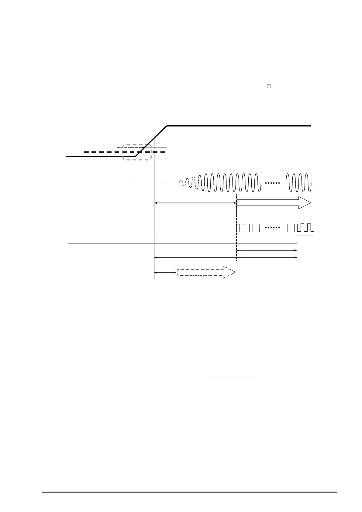
Figure 12 Power supply initial sequence
10.2. Precautions for power ON / OFF
1: To ensure that the power-on reset works at the initial power-on keep V
DD
=V
BAT
=GND for 10 seconds or more before
V
DD
= ON.
2: Initial power-on tR1 is a necessary condition for enabling power-on reset.
If this condition is not satisfied, power-on reset may not work. As a result, the time accuracy and current consumption
may not meet the specifications. Please reset by software. See 18.2 Software Reset.
3: When fluctuation of V
DD
is out of specifications, tF or tR2, it may be occur the followings, a momentary stop of crystal
oscillation, a set of VLF by V
OUT
voltage drop lower than V
CLK
and so on.
4: The timing at which the I
2
C-Bus interface is enabled differs in when the initial power of V
DD
is turned on and when
V
DD
is turned on from backup mode.
See the tCL and tCU specifications in the chart below.
5: These specifications don't mean a noise characteristic of a power supply of RTC.
Do not use amplitude signal output from a signal generator etc, as a power source.
After 30 ms progress, Readout of VLF is possible.
At the time of VLF=1: After a t_str wait, initial setting is necessary.
At the time of VLF=0: Register access is possible.
However, clock updating is invalid while t_str.