3. Terminal description
RX8130CE Jump to Top / Bottom
ETM50E-07 Seiko Epson Corporation 7
3. Terminal description
3.1. Terminal connections
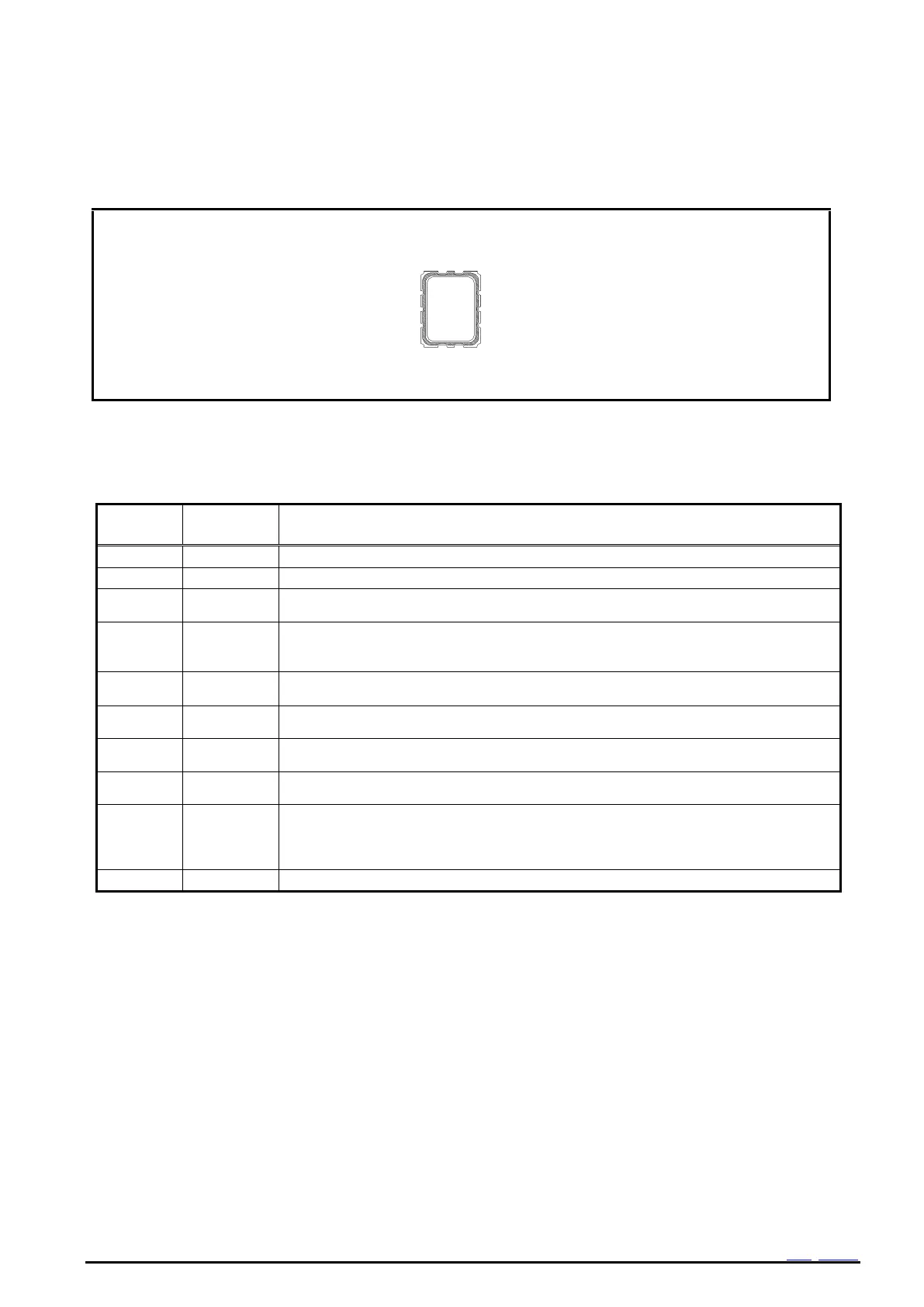
Figure 2 Package
3.2. Pin Functions
Table 1 Pin Description
Data input and output pin.
Frequency output pin with output control function. (CMOS)
Output frequency can be selected as 32.768k Hz, 1024 Hz, 1 Hz.
Even in the backup mode, this pin can operate. In case of V
DD
voltage drop detection, a
reset signal is outputted. (N-ch open drain)
In case of V
DD
voltage rise detection, it releases the reset signal after 60ms.
Interrupt output by Alarm and Timer events.(N-ch open drain)
This pin can output even a backup mode.
This is a power-supply pin for the internal logic.
This is an interface power supply pin.
Connect the same power supply as the MCU.
Internal voltage output pin.
Connect smoothing capacitor of 1.0uF
This is a power supply pin for backup battery.
This is a pin to connect a large-capacity capacitor, a secondary battery, and a primary
battery.
In a backup mode, the voltage is supplied inside by this pin.
Note: Connect a bypass capacitor rated at least 0.1μF between power supply pins and GND pin.
Note: Input pins are able to input up to 5.5V regardless of V
IO
applied voltage.
Note: Open drain pins are able to Pull-up to 5.5V regardless of V
IO
applied voltage.
Note: Use the FOUT, /RST, /IRQ terminals as Open when not in use. Don't connected to GND or V
DD