10. Interface timing when power is turned ON / OFF
RX8130CE Jump to Top / Bottom
ETM50E-07 Seiko Epson Corporation 16
10.3 V
DD
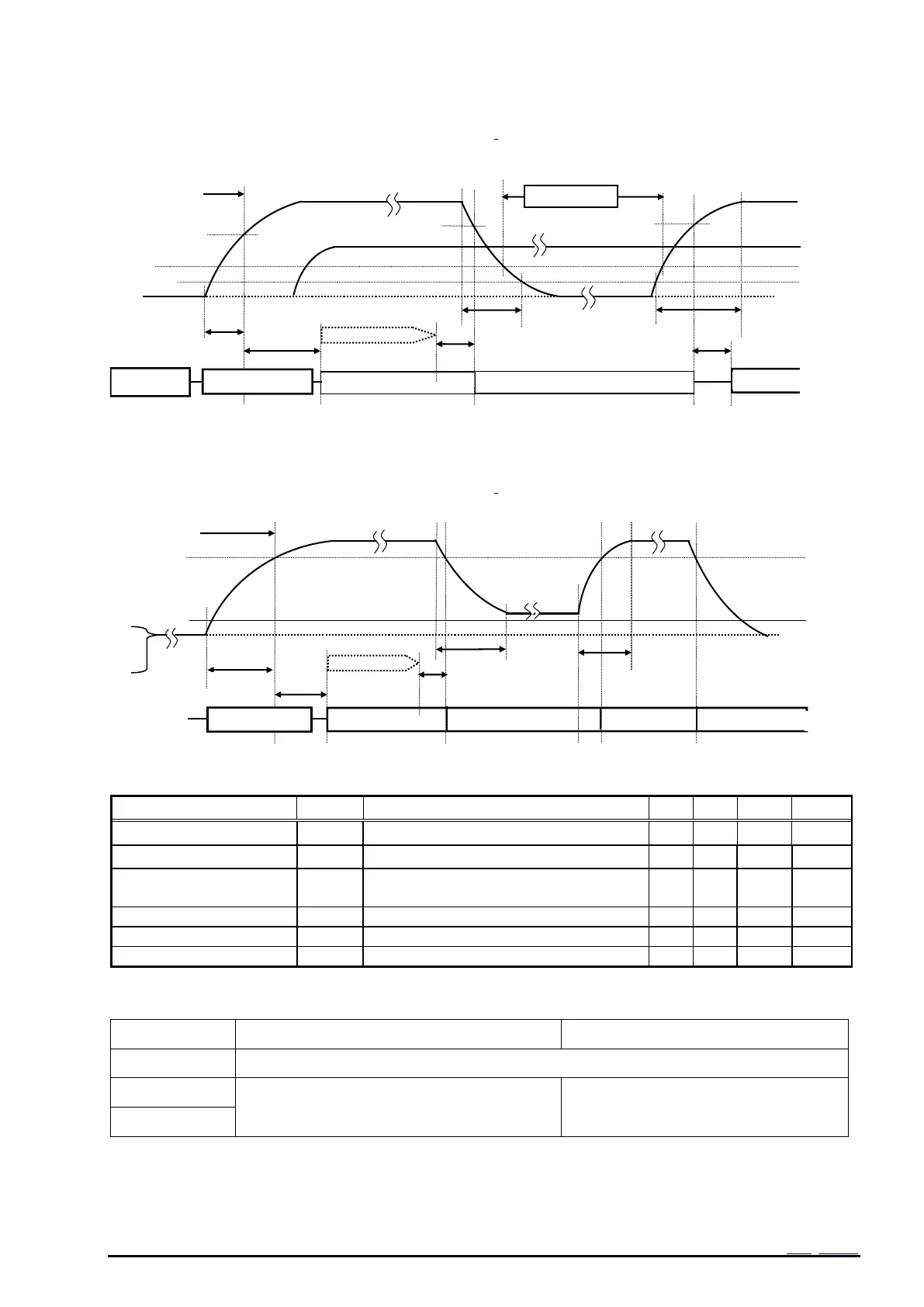
ON / OFF when using power switching (INIEN = 1)
See "4.1. Examples of power supply connection" Circuit EX1, 2, 3.
Figure 13 Power-On sequence1
10.4 V
DD
ON / OFF when power switching is not used (INIEN = 0)
See "4.1. Examples of power supply connection" Circuit EX4.
Figure 14 Power-On sequence2
Table 11 Power supply characteristics
From GND to VDD = +VDET11
VDD = +VDET11 to Access start
The time from the end of I
2
C access to the
disable of I
2
C
Time to restore V
DD
to operating voltage
VDD=+VDET1x to Access start
tR1, tR2, and tF specify that there is no voltage fluctuation faster / slower than the Min / Max specifications within the specified section.
The risk when specifications were not satisfied, refer to the following.
Risk of fast fluctuations
Risk of slow fluctuations
Power-On-Reset doesn't occur.
The FOUT waveform disappears momentarily,
and clock time is momentarily delayed.
A data of RTC loss. A set of VLF.
V
DD
and V
BAT
in Figures 13 and 14 are the voltages of V
DD
and V
BAT
pins of RX8130CE.
Regarding access to the clock register after the initial power-on,
, See "10.1 restrictions of I2C interface in the initial power on". The clock from FOUT is outputted after tCU.
When status of V
DD
= V
BAT
= GND doesn't keep more than 10seconds before initial power-on, the Power-On-Reset may not work even if
the tR / tF specifications are satisfied.