13. Overview of Functions and Registers
RX8130CE Jump to Top / Bottom
ETM50E-07 Seiko Epson Corporation 20
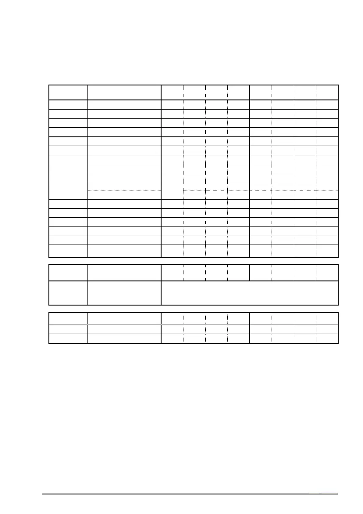
13.2. Register Table
13.2.1. Register Table
Table 12 Register Table
User Register
32 bits ( 4-word x 8 bit )
After the initial power-up (from 0V) or in case the VLF bit returns "1" , make sure to initialize all registers, before
using the RTC.
Be sure to avoid entering incorrect date and time data, as clock operations are not guaranteed when the data or time
data is incorrect.
The TEST bit is used by the manufacturer for testing. Be sure to set "0" for this bit when writing. Be sure to write "0"
by initializing before using the clock module. Afterward, be sure to set "0" when writing
“0” means that writing is invalid and the read value is always 0.
Any bit marked with "" is a RAM bit that can be used to read or write any data.
User Register is a free register which can be used as user RAM.
The above table shows only the user registers. Due to functional reasons, RTC has different registers not mentioned
above table which are programmed by the manufactorer. Please make sure to only access above mentioned user
registers.
“-“ bit is TEST bit. As initialization “0” should be set and be kept “0”.