-
FIGURE
Frontispiece
1-1.
2-1.
2-2.
2-3.
2-4.
2-5.
2-6.
2-7.
2-8.
2-9.
2-10.
2-11.
2-12.
2-13.
2-14.
2-15.
2-16.
2-17.
3-1.
3-2.
3-3.
3-4.
3-5.
3-6.
4-1.
4-2.
List of Figures
TITLE
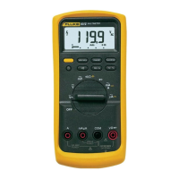
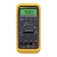
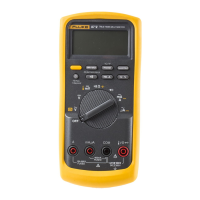
8050A Digital Multimeter
..........................................
.
8050A Dimensions
................................................
.
Controls, Indicators, and Connectors
................................
.
Liquid Crystal Display
.............................................
.
AC/
DC
Voltage Operation
.........................................
.
AC/DC
Current Operation
.........................................
.
Resistance Operation
..............................................
.
Conductance Operation
............................................
.
Diode Test Operation
.............................................
.
Relative Operation
.......
.-
........................................
.
dB Voltage Operation
.............................................
.
Circuit Loading Error
.............................................
.
Calculating Burden Voltage
Error
...................................
.
Transistor Beta Test Fixture
........................................
.
dB Circuit Gain
or
Loss Measurements
..............................
.
Waveform Comparisons
...........................................
.
Crest Factor
.....................................................
.
Total RMS Value
.................................................
.
Measuring Amplifier Bandwidth
•....................................
8050A Functional Block Diagram
...................................
.
A/D
Converter
...................................................
.
A/D
Converter Waveforms
........................................
.
Microcomputer Simplified Block Diagram
...........................
.
Signal Conditioning
...............................................
.
RMS Converter
..................................................
.
Display PCB Access
...............................................
.
Calibration Adjustment Locations
...................................
.
v
PAGE
Vl
1-6
2-2
2-4
2-5
2-6
2-7
2-8
2-9
2-10
2-11
2-13
2-14
2-15
2-17
2-18
2-19
2-19
2-20
3-3
3-4
3-5
3-6
3-7
3-9
4-3
4-9