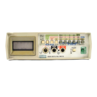
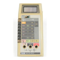
3-1. INTRODUCTION
3-2.
The theory
of
operation
of
the
8050A
is
discussed
on two levels. First, the Functional Description discusses
the operation
of
the
DMM
in terms
of
the functional
relationships
of
the major circuits.
Second,
the Circuit
Description presents a more detailed discussion
of
the
major circuits. Both levels are illustrated by block
diagrams and simplified schematics in this section and the
schematic diagrams in
Section
7.
3-3. FUNCTIONAL DESCRIPTION
3-4.
The major circuits
of
the
8050A
are shown in the
functional block diagram in Figure
3-1.
The range and
function switches route the unknown input signal
through the signal conditioners. The signal conditioners
develop a de voltage
at
the input to the
a/
d converter
that
is
proportional to the unknown input signal. The
a/
d
converter,
working
in
conjunction
with
the
microcomputer, converts the de analogue
of
the unknown
input signal to a digital value. The microcomputer
processes the digital value and displays the result on the
LCD.
3-5.
CIRCUIT DESCRIPTION
3-6.
The following paragraphs describe each
of
the
major circuits in detail.
3-7.
AID
Converter
3-8.
The
a/d
converter in the
8050A
uses the dual slope
method of conversion.
In
this method, the voltage
analogue
of
the
input
signal
(proportional
to
the
unknown input signal)
is
allowed to charge a capacitor
(integrate) for
an
exact length of time. The capacitor
is
then discharged by a reference voltage. The length
of
time
required for the capacitor to discharge
is
proportional to
the unknown input signal. The microcomputer measures
the discharge time and displays the result. The following
Section
3
Theory of Operation
paragraphs discuss the actual
a/
d conversion in more
detail.
3-9.
The microcomputer controls the
a/
d converter via
CMOS
switches. Figure
3-2
shows the simplified circuits
formed during the major periods
of
a/
d conversion
cycles. Figure
3-3
is
a timing diagram that shows the
a/
d
converter cycle resulting from three different
input
signals. Assume in reading the following paragraphs
that
the
DC
V function and the
2V
range are selected, and the
DMM
is
nearing the end
of
the Autozero period in its
conversion cycle.
3-10.
As
Part
A in Figure
3-2
shows, the
CMOS
switches
Ul8B
and
Ul9A
are closed, providing voltage
levels that allow
C8
and
C33
to store the offset voltages
of
the buffer, integrator, and comparator.
CMOS
switches
Ul8D
and
Ul9B
connect the flying capacitor, C7, to a
reference voltage.
Since
the V function
is
selected,
C7
is
charged by the
a/
d converter reference voltage source. At
the end
of
the Autozero period, C7
is
fully charged,
C8
and C33 are charged up to the offset voltages, and the
comparator output (CM) is near a threshold level.
3-11.
Assume that
an
input
of
-1.0000V
de
is
present
at
the
DMM
input(firstset
of
waveforms in Figure3-3). The
microcomputer starts the Integrate command (INT)
at
the same time that it ends the AZ command. The
a/
d
converter circuit
is
switched to the configuration shown in
Figure 3-2, Part
B.
CMOS
switch
Ul8A
connects the
output
of
the signal conditioners to the input terminal
of
the buffer.
For
the
2V
range, the microcomputer selects
the
Xl
gain
in
the buffer, and the input from the signal
conditioner
is
applied to the buffer and integrator in
series. The integrator begins to charge C9. The instant
that the charge on
C9
shifts from its initial level, the
comparator toggles, and its Compare output (CM) goes
to a steady level.
Since the unknown input to the
DMM
is
3-1