FC6A S
ERIES
MICROS
MART
U
SER
’
S
M
ANUAL
FC9Y-B1722 2-133
2: P
RODUCT
S
PECIFICATIONS
■ Output Specifications
Output Internal Circuit
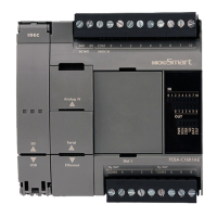
Type No. FC6A-F2M1, FC6A-F2M4 FC6A-F2MR1, FC6A-F2MR4
Output
Type and
Output
Range
Digital Output
Transistor protection source output
(12V DC output)
Relay output
Analog Output 4 to 20 mA ―
Load
Digital Output Max 40 mA (12V DC) ―
Analog Output 550 Ω or higher ―
Relay Output ―
5 A 250V AC (resistive load)
5 A 30V DC (resistive load)
3 A 250V AC (inductive load cosφ=0.4)
3 A 30V DC (inductive load L/R=7 ms)
Load Type Resistive load Resistive load/inductive load
DA
Conversion
Analog Output Settling Time 80 ms ―
Digital Output Delay Time
Turn OFF time: 10 ms
Turn ON time: 5 ms
―
Total Output System Transfer Time
Analog output: Settling time + input sampling time (100 ms)
Digital output/relay output: Output delay time + proportional cycle (1 to 120 s)
Output
Error
Maximum Error at 25°C ±0.5% of full scale
Temperature Coefficient ±0.01% of full scale/°C
Output Ripple ±0.2% or less of full scale
Overshoot 0%
Data
Digital Resolution 1,000 steps (10 bits)
Input Type and Input Range 0.0016 mA (4 to 20 mA)
Monotonicity Yes
Current Loop Open Not detectable
Noise
Resistance
Maximum Temporary Deviation
during Electrical Noise Tests
±4% or less of full scale
Recommended Cable for Noise
Immunity
Current/voltage: Pair shielded cable
Crosstalk 1 LSB
Isolation
Between Output and Power Circuit Transformer isolated
Between Output and Internal
Circuit
Photocoupler isolated
Effect of Improper Output Connection No damage
Selection of Analog Output Signal Type Using programming software
Calibration or Verification to Maintain Rated
Accuracy
Not possible
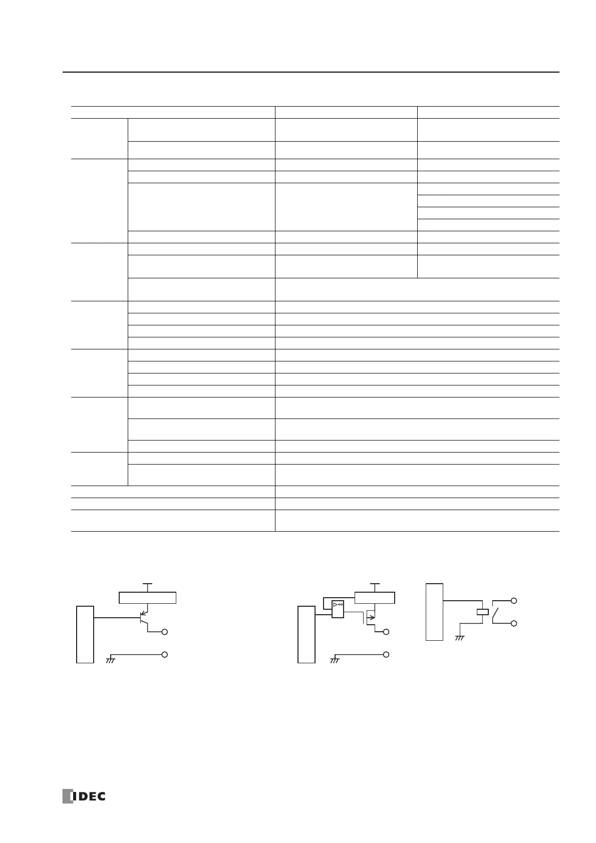
FC6A-F2M1, FC6A-F2M4
(non-contact voltage output (to drive SSRs))
FC6A-F2M1, FC6A-F2M4
(current output)
FC6A-F2MR1, FC6A-F2MR4
Output Circuit
+
–
Short Circuit Protection Circuit
Output Circuit
+
–
Current Detection
Output Circuit
+
–
 Loading...