GB - 15
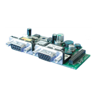
Control circuit
2.1.5.2 Assignment of the terminal strip X2A
1
2
3
4
5
6
7
8
9
10
11
12
13
14
15
16
17
18
19
20
21
22
23
24
25
26
27
28
31
32
29
30
PIN Name Description Specications
1 0V Digital mass; Reference potential for digital inputs/outputs and U
in
2 U
in
Input external voltage supply U=24 VDC +20 %/-15 %
I
max
=400 mA
3 0V like pin 1
4 U
out
Voltage output for the control of the digital
inputs
U=24 VDC ±25 %
I
max
=100 mA
5 RST reset
8 digital inputs according to IEC61131-2 type
1
„0“ = -3…5 VDC
„1“ = 15…30 VDC
Scan time ≤ 2 ms
6 ST
1)
Control release
7 R Direction of rotation re-
verse
8 F Direction of rotation for-
ward
9 I2 Digital input 2
10 I1 Digital input 1
11 I4 Digital input 4
12 I3 Digital input 3
13 O2 Digital output 2 2 digital transistor outputs PNP
U=24 VDC ±25 %
I
max
=50 mA ohmic load for O1+O2
max switching frequency = 250 Hz
14 O1 Digital output 1
15 0V like pin 1
16 CRF Reference voltage for
setpoint potentiometer
10 VDC +5 %; I
max
= 4 mA
17 AN1- -Analog input 1 adjustable:
0…±10 V (R
i
=55 kΩ)
0…±20 mA (R
i
=250 Ω)
4…20 mA (R
i
=250 Ω)
Resolution: 10 Bit + sign
Scan time ≤ 2 ms
18 AN1+ +Analog input 1
19 AN2- -Analog input 2
20 AN2+ +Analog input 2
further on next side
 Loading...