Troubleshooting
2-94
2.11.24 True RMS converter and filter tests
Test 410.1 — True RMS converter
Type
Pass/Fail
Fault message TRMS
Description The REFHI line is tied to pin 1 of U420 and buffered to form BUFF. BUFF is routed through
R493, K403, K401, input protection, and Q421 is tied to the input buffer Q418 and U423. The
buffered BUFF signal (AMP IN) is tied to the FWR, and, being positive, follows the non-invert-
ing, X1 path R452, Q412, Q411, U417, R453, U410, Q404, and U419 to pin 15 of the TRMS
converter U420. The output of U420 is tied to U414 pin 6 through R219, and the output of U414
is tied to the A/D buffer through buffer U403, R434, R462, and U222. The A/D buffer is config-
ured for X1 gain.
Drawing reference Analog Board; 2002-100
Components U410, U417, U420, U423, and associated components.
Bit patterns
Test 411.1 — True RMS filter
Type Pass/Fail
Fault message TRMS filter
Description REFHI is tied to pin 1 of U420 and buffered to form BUFF. BUFF is routed through R493,
K403, K401, input protection, and Q421 is tied to the input buffer Q418 and U423. The buffered
BUFF signal (AMP IN) is tied to the FWR, and, being positive, follows the non-inverting, X1
path R452, Q412, Q411, U417, R453, U410, Q404, and U419 to pin 15 of the TRMS converter
U420. The output of U420 is tied to filter R435, R446, R447, C433, C434, C432, and U426
through U413. The output of the filter is tied to U414 pin 5, and the output of U414 is tied to the
A/D buffer through buffer U403, R434, R462, and U222. The A/D buffer is configured for X1
gain.
Drawing reference Analog Board; 2002-100
Components U413, U417, U419, U420, U423, U426, and associated components.
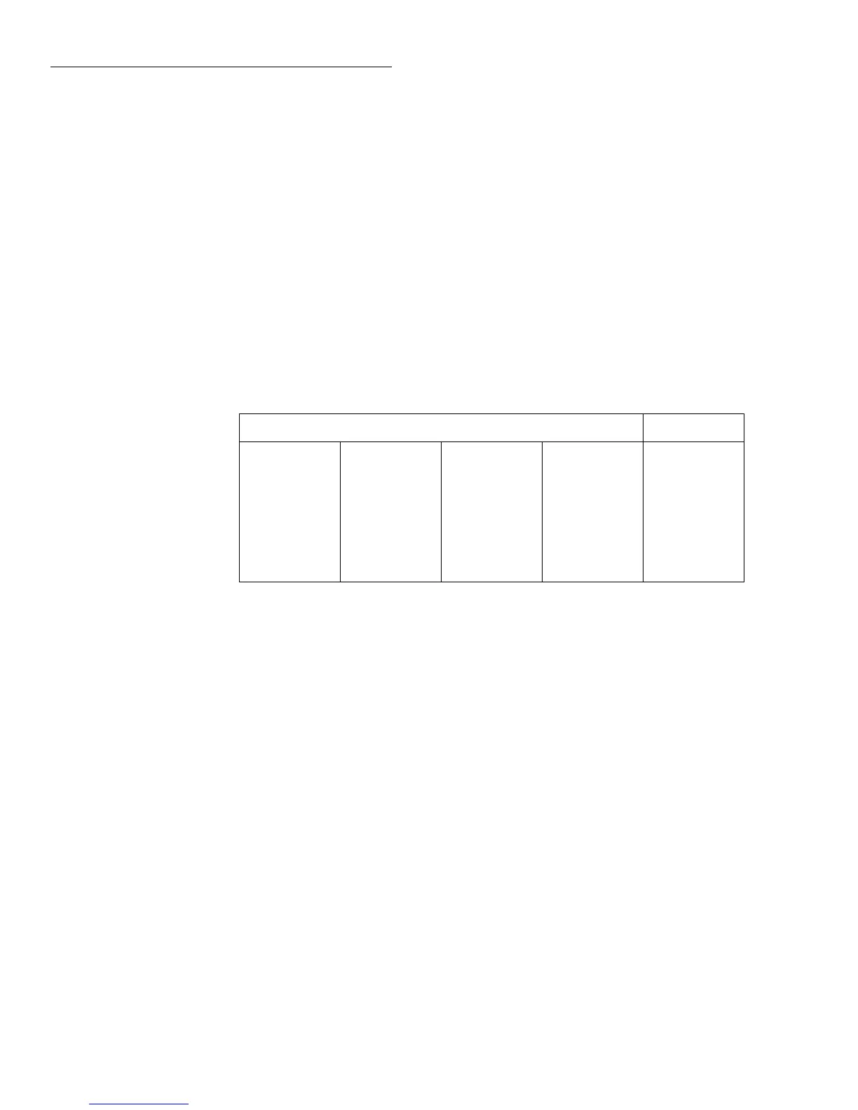
Bit pattern* Register
—U400—
01011010
—U811—
00001101
—U224—
00010111
—U432—
10000000
—U810—
00000011
—U206—
01110000
—U203—
10001110
—U411—
10111001
—U809—
11100111
—U207—
11001111
—U221—
11101001
—U406—
10101110
AD_STB
MUX_STB
R1_STB
R2_STB
*Bits associated with register IC terminals as follows:
QQQQQQQQ
87654321 87654321 87654321 87654321
IC pins: Q8=11, Q7=12, Q6=13, Q5=14, Q4=7, Q3=6, Q2=5, Q1=4.

 Loading...