Troubleshooting
2-84
2.11.21 Front end X1, / 100, /500 tests
Test 407.1 — Front end 2V range
Type
Pass/Fail
Fault message
Front end 2V range
Description
The REFHI line is buffered by U255 to create REFBUF and is tied to pin 1 of U420 and then
buffered to form BUFF. BUFF is routed through R493, K403, K401, input protection, and Q421
is tied to the input buffer Q418 and U423. The buffered BUFF signal (AMP IN) is tied to the
FWR, and, being positive, follows the non-inverting, X1 path R452, Q412, Q411, U417, R453,
U410, Q404, and U419 to pin 12 of U414. The output of U414 is tied to the A/D buffer through
buffer U403, R434, R462, and U222. The A/D buffer is configured for X1 gain.
Drawing reference
Analog Board; 2002-100
Components
Q418, U410, U417, U419, U420, U423, and associated components.
Bit patterns
Test 407.2 — Front end 200V range
Type
Pass/Fail
Fault message
Front end 200V range
Description
The REFHI line is buffered by U255 to create REFBUF and tied to pin 1 of U420 and then buffered
to form BUFF. BUFF through R493 is tied to NET1 pin 1 (R488). The divided voltage (/100) at
R488 pin 4 is tied to the input buffer Q418 and U423 through U428 and Q422. The buffered sig-
nal AMP IN is tied to the FWR, and, being positive, follows the non-inverting, X10 path R452,
Q413, Q411, U417, R453, U410, Q404, and U419 to pin 12 of U414. The output of U414 is tied
to the A/D buffer through buffer U403, R434, R462, and U222. The A/D buffer is configured for
X1 gain.
Drawing reference
Analog Board; 2002-100
Components
Q418, U410, U417, U419, U420, U423, and associated components.
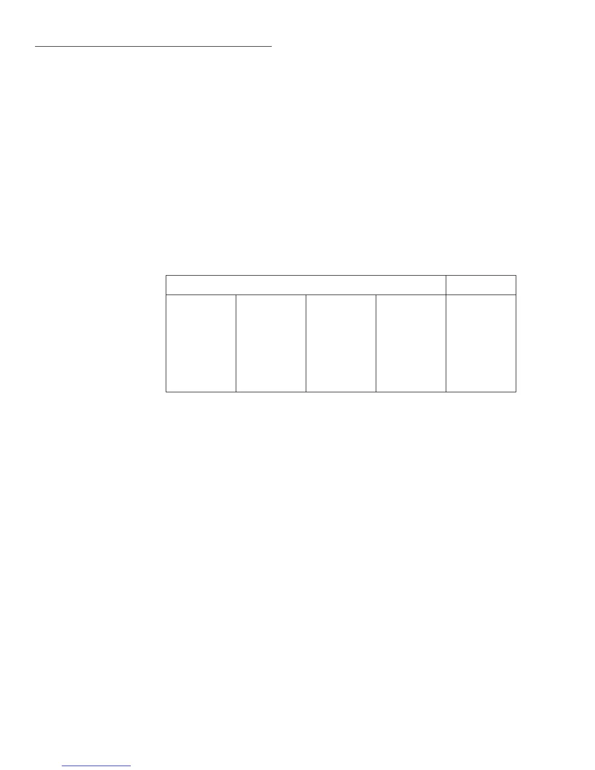
Bit pattern* Register
—U400—
01110100
—U811—
00001101
—U224—
00010111
—U432—
10000000
—U810—
00000011
—U206—
01110000
—U203—
10001110
—U411—
11111000
—U809—
11100111
—U207—
11001111
—U221—
11101001
—U406—
11101110
AD_STB
MUX_STB
R1_STB
R2_STB
*Bits associated with register IC terminals as follows:
QQQQQQQQ
87654321 87654321 87654321 87654321
IC pins: Q8=11, Q7=12, Q6=13, Q5=14, Q4=7, Q3=6, Q2=5, Q1=4.
 Loading...