Troubleshooting
2-80
2.11.20 Sample and hold tests
Test 406.1 — Read DAC V for sample and hold test 406.6
Type
Circuit Exercise
Fault message None
Description DAC U433 and op amp pair U430 are set up to generate -1.13 VDC at PRECOMP+ and tied to
ACF through R491 and U412. ACF is tied to pin 7 of multiplexer U414. The output of the mul-
tiplexer is tied to the A/D through buffer U403, ACV/A input to U222, and the A/D buffer in X1
gain configuration. The value of the DAC voltage is measured and stored. This value will also
be applied to the circuit in tests 406.2 and 406.3. In this manner, the applied value to the circuit
and the output value (SELFTEST OUT) can be compared to check for circuit accuracy in test
phase 406.6.
Drawing reference Analog Board; 2002-100
Bit patterns
Test 406.2 — Sample and hold output (-1.13V)
Type Circuit Exercise
Fault message None
Description DAC U433 and op amp pair U430 are set up to generate -1.13 VDC at PRECOMP+ and tied to
ACF through R491 and U412. ACF is buffered to AMP IN through U428, Q422, and ACV buff-
er. AMP IN is tied through U425, to inverting X5 gain U426, R466, and R465. The SELFTEST
signal causes one-shot U402 to output a 5µs low pulse, turning U425 and Q414 ON for 5µs. The
value from inverter U426 is stored on C439 and applied to buffer Q409. SELFTEST OUT is the
value on C439 and the V
GS
value of Q409. This signal is applied to multiplexer U414 pin 11.
The multiplexer output is tied to the A/D through buffer U403, ACV/A input to U222, and the
A/D buffer in X1 gain configuration.
Drawing reference Analog Board; 2002-100
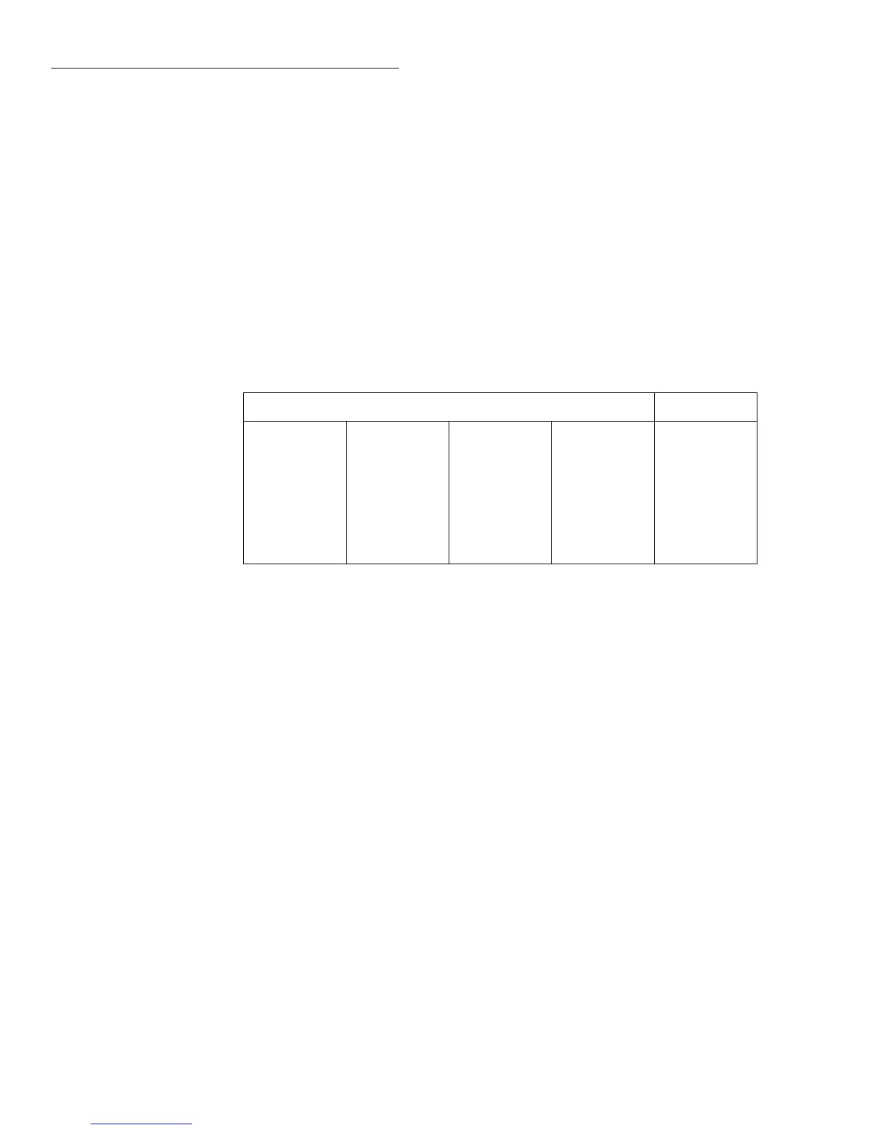
Bit pattern* Register
—U400—
01011100
—U811—
00001101
—U224—
00010111
—U432—
01100100
—U810—
00000011
—U206—
01110000
—U203—
10001110
—U411—
11111011
—U809—
11100111
—U207—
11001111
—U221—
11101001
—U406—
01001111
AD_STB
MUX_STB
R1_STB
R2_STB
*Bits associated with register IC terminals as follows:
QQQQQQQQ
87654321 87654321 87654321 87654321
IC pins: Q8=11, Q7=12, Q6=13, Q5=14, Q4=7, Q3=6, Q2=5, Q1=4.