Troubleshooting
2-78
Test 405.6 — Absolute value X10 gain (inverting)
Type
Pass/Fail
Fault message Absolute value gain = 10
Description DAC U433 and op amp pair U430 are set up to generate -0.210 VDC at PRECOMP+. This signal
has the same path to the FWR as test 405.2. However, in this test with AMP IN negative,
NETOUT from U417, the ZERO CROSSING amp, and the COMP- signal that is tied to com-
parator U408 select the inverting path for the AMP IN signal. The minus AMP IN path with
FWR X10 is through R452, U418, U410, Q404, and U419 to pin 12 of multiplexer U414. The
output of the multiplexer is tied to the A/D through buffer U403, ACV/A input to U222, and the
A/D buffer gain is X1.
Drawing reference Analog Board; 2002-100
Components U403, U408, U412, U414, U417, U419, U430, U433, and associated components.
Bit patterns
Test 405.7 — Large negative DAC V for X10 gain comparison
Type Circuit Exercise
Fault message None
Description DAC U433 and op amp pair U430 are set up to generate -0.490 VDC at PRECOMP+. This signal
follows the same path as test 405.1. This test has the same purpose as test 405.1, but the new test
value is used for 405.8.
Drawing reference Analog Board; 2002-100
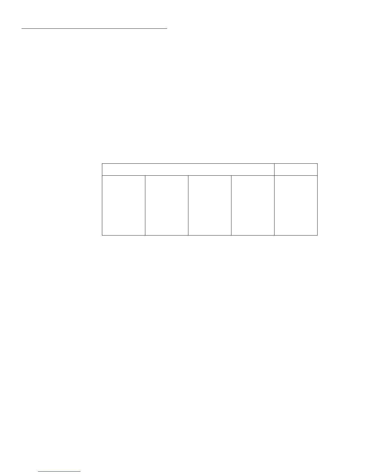
Bit pattern* Register
—U400—
01011100
—U811—
00001101
—U224—
00010111
—U432—
01111011
—U810—
00000011
—U206—
01110000
—U203—
10001110
—U411—
11111111
—U809—
11100111
—U207—
11001111
—U221—
11101001
—U406—
01001111
AD_STB
MUX_STB
R1_STB
R2_STB
*Bits associated with register IC terminals as follows:
QQQQQQQQ
87654321 87654321 87654321 87654321
IC pins: Q8=11, Q7=12, Q6=13, Q5=14, Q4=7, Q3=6, Q2=5, Q1=4.