sowe output is lOV, but this value is divided to 1V and O.lV
by a voltage divider made up of elements of R304. Q302
buffers the output of U304 since R304 will draw lOmA.
Only a single voltage source value is used for a given range,
with the value being selected by the appropriate relay con-
tacts. For the 2MR range, however, all relay contacts are
open and a 1p.A current is sourced through the precision
90OkR resistor R303 and feedback element R322.
6.3.5 Zero Check
The zero check mode provides a means for determining and
cancelling offsets internal to the instrument. The exact con-
figuration of the zero check circuitry will depend on the
selected function.
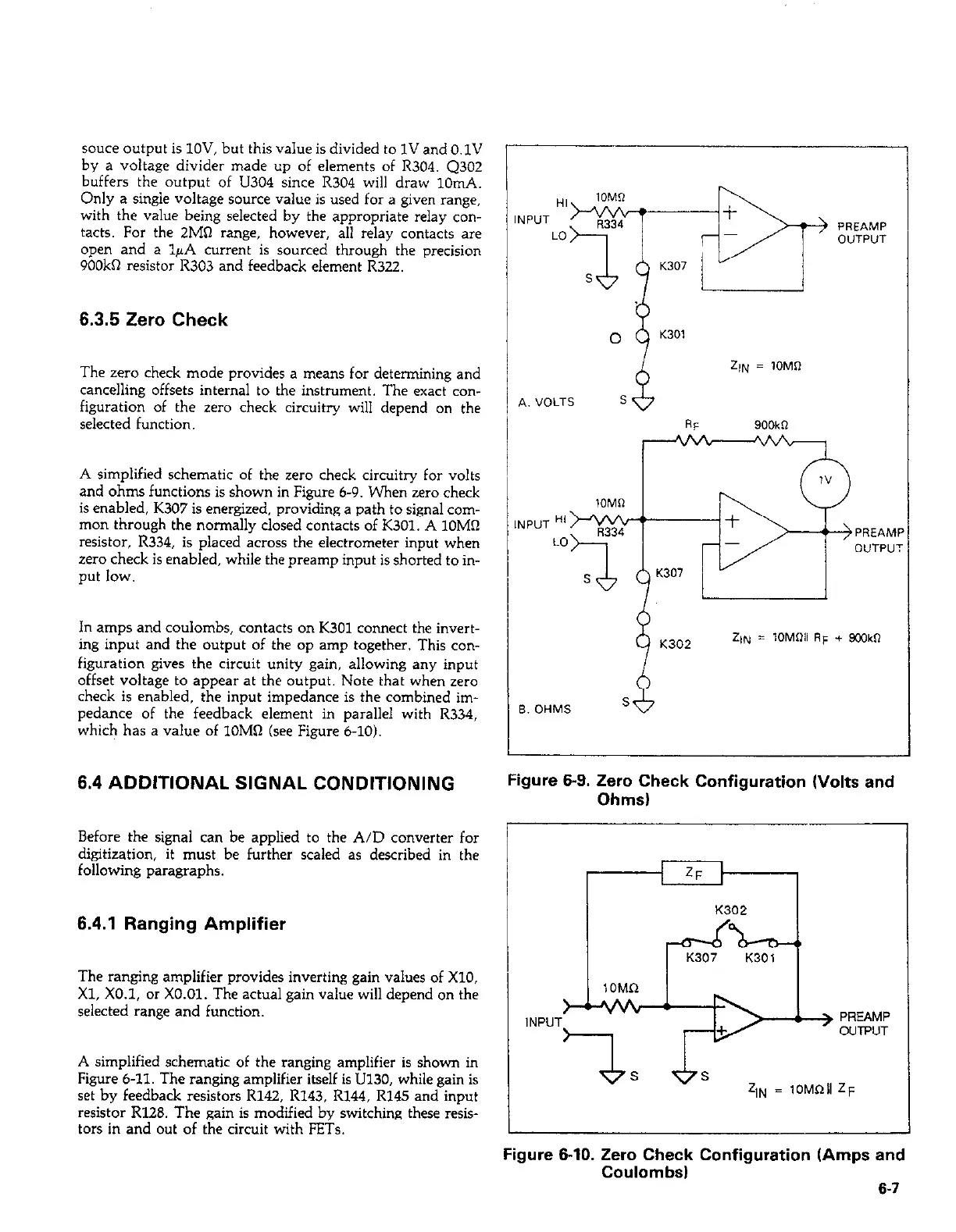
A simplified schematic of the zero check circuitry for volts
and ohms functions is shown in Figure 6-9. When zero check
is enabled, K307 is energized, providing a path to signal com-
mon through the normally closed contacts of K301. A 1OMR
resistor, R334, is placed across the electrometer input when
zero check is enabled, while the preamp input is shorted to in-
put low.
In amps and coulombs, contacts on K301 connect the invert-
ing input and the output of the op amp together. This con-
figuration gives the circuit unity gain, allowing any input
offset voltage to appear at the output. Note that when zero
check is enabled, the input impedance is the combined im-
pedance of the feedback element in parallel with R334,
which has a value of 1OMR (see Figure 6-10).
r
I’
ZIN = lOM0
NPUT ”
LO
PREAMl
OVTP”:
K302
2,~ = ioMl,if flF + %3,kR
6.4 ADDITIONAL SIGNAL CONDITIONING
Figure 6-9. Zero Check Configuration (Volts and
Ohms)
Before the signal can be applied to the A/D converter for
digitization, it must be further scaled as described in the
following paragraphs.
6.4.1 Ranging
1 Amplifier
The ranging amplifier provides inverting r-‘- ---‘-~-- mr “**
I
x1, x0.1, ^_ vn ,v l-l... -^L___l ^^i_ ..^I_.^
selected r
K302
I
A simplified schematic of the ranging amplifier is shown in
Figure 6-11. The ranging amplifier itself is U130, while gain is
set by feedback resistors R142, R143, Rl44, R145 and input
resistor R128. The gain is modified by switching these resis-
tors in and out of the circuit with FETs.
Figure 6-10. Zero Check Configuration (Amps and
Coulombs)
6-7