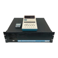
960L Multi-Channel Digital Effects System Service Manual
7-22
so equilibrium is achieved when U14 outputs are somewhat below the Vbe of Q3, although not quite 0. A
slight positive equilibrium point is desirable to accomodate the asymmetrical tolerances of the +/-12V
system supplies as well as the asymmetrical output capability of the OPA2134, with the objective of
maximizing the voltage range available for the audio signal. In addition to compensating for D/A bias
current, the dc feedback also compensates for the FILTR compliance voltage, which requires another
0.4mA through each bias resistor. The presence of R47 and R51 at the summing nodes increases the noise
gain of the I/V converter stages, but the effect decreases as the resistance increases, so large values are
used. Q4 derives the bias current from VB, which is about +30Vdc. R47 (and R51) develop a voltage of
around 2.4mA*10k=24V, so the collector of Q4 operates at about 28V, filtered by C93. The bias voltage at
this point is common mode, so any noise present is rejected to a high degree by the differential signal
stages.
By eliminating dc bias in the output of the I/V converters, their usable range is available for developing a
large audio signal, which is favorable for achieving a high signal-to-noise ratio. Full-scale ac signal voltage
at U14.1 is 9.8Vpeak (19dBu).
The sigma-delta current from the D/A has substantial components at frequencies well above the audio
band, and C121, C95, and C94 are important for accommodating and reducing this high-frequency content
in the I/V conversion.
Filter
U22 and associated components form a 2-pole multiple-feedback active filter that further reduces the non-
audio content of the analog output. This filter has a characteristic lying between Bessel and Butterworth,
with a -3dB frequency around 120kHz. The overall filter characteristic of the channel is designed to have a
flat frequency response well within 0.5dB out to 40kHz and to exhibit a transient response consistent with
the enhanced temporal/spatial resolution available at the double-speed 88.2/96kHz sampling rates. Mid-
band gain is around 0.45 (-6.9dB), producing a full-scale CH1 signal of about 18dBu (8.7Vpeak).
Output Driver
The output of the filter is ac-coupled by C157 to U26, a monolithic transformerless differential output line-
driver (DRV134). The differential output is fed back via dc blocking capacitors C165,C166 to its sense
inputs. The driver has an output impedance of 50ohms and a nominal voltage gain of 6dB when driving
600ohms. With this low output impedance, the output level with and without a 600ohm load (dBm vs. dBu)
differs by <1dB. Full-scale output is nominally +24dBm, and the transformerless characteristic makes signal
level insensitive to load imbalance (high common-mode output impedance). C181 placed directly across the
50-ohm differential output forms the final pole in the overall filter characteristic.
Power for U26, +/-VCC, is derived from capacitive charge pumps which augment the +/-12V system
supplies to +/-18V nominal, unregulated (sheet 7, see below). The higher voltage accommodates a modest
common-mode output voltage arising from some degree of load imbalance or an equivalent external source
of output common-mode voltage, while providing the supply current necessary at program peaks. With a
perfectly balanced load, each output leg referred to common is +18dBu full-scale, 8.7Vpeak, around 5-6V
below clipping. The output can therefore tolerate up to several volts of peak common-mode voltage,
regardless of how it arises.
Note that the output driver cannot produce full +24dBm level if the output is wired for single-ended
unbalanced operation with one leg grounded, as this would result in a common-mode voltage of 18dBu,
corresponding to a peak output voltage greater than 17V, beyond clipping level. If grounded unbalanced
wiring is employed, the maximum digital signal that can be accommodated is around -2 dBFS.
Mute Relay
RY1 in the normally-closed position mutes the differential output by grounding pins 2 and 3 of XLR
connector J2. When energized under software control, RY1 connects J2 to the active output circuitry.
 Loading...