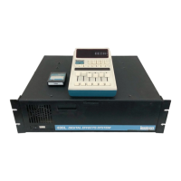
960L Multi-Channel Digital Effects System Service Manual
7-26
7 SDO2 INPUT TMIX Octal data. Received from TMIX2 Octal 8. Octal selection is
determined by the octal select field in the FPGA control register(see
register description for details)
84 SDO3 INPUT TMIX Octal data. Received from TMIX2 Octal 9. Octal selection is
determined by the octal select field in the FPGA control register(see
register description for details)
9 SDO4 INPUT TMIX Octal data. Received from TMIX2 Octal 10. Octal selection is
determined by the octal select field in the FPGA control register(see
register description for details)
10 SDO5 INPUT TMIX Octal data. Received from TMIX2 Octal 11. Octal selection is
determined by the octal select field in the FPGA control register(see
register description for details)
Audio Control
44 DEEPMH OUTPUT Deemphasis control. Enabled when asserted(1).
39 RLY_MUTE/ OUTPUT Relay Mute Control. Analog outputs are muted when asserted(0)
27 DAMUTE OUTPUT DA Mute. Digital output from DA is muted when asserted(1)
28 DAC_RST/ OUTPUT DAC reset. All DACs’ are reset when asserted(0).
26 96K_EN OUTPUT 96K sample rate enable. DACs’ operate in 2x(88.2/96K) sampling mode
when asserted(1).
Charge Pump Support
38,36,
58
VBOSCU/,VBOSCD/,
VCCOSC
OUTPUT Charge pump clock signals
FPGA Support
32 MODE INPUT MODE - Serial download interface mode signal. Nomimally zero for
loading from external SPROM
55 PROG/ INPUT FPGA Program. 0 : causes the FPGA to reload its program from the
external SPROM.
73 CCLK OUTPUT CCLK . Serial PROM clock signal
53 DONE OUTPUT FPGA DONE - Asserted when FPGA program cycle has completed.
41 INIT/ OUTPUT FPGA serial download initialization signal.
71 DIN INPUT FPGA configuration data from SPROM
15,16,
17
TDI,TCK,TMS INPUT JTAG Interface. Not used
75 TDO OUTPUT JTAG Interface. Not used
Power Supply
Power conditioning for the Analog Output card involves local filtering and regulation of supplies from the
backplane, as well as the production of boosted voltages for special purposes.
The main 5VD from the backplane is used by the fpga and the digital sections of the D/A converters.
The 12V supplies from the backplane (+12VSUP/-12VSUP) are filtered by FB4/FB1 and associated
capacitors to supply +/-12V to the analog op-amps. +12VSUP also supplies U3 through a string of 5
dropping diodes to provide regulated +5VA for the D/A converters, which consume 8 x 15=120mA
maximum. Diodes D8, D9 prevent large differences from existing between the 5V pins of the converters.
U4 develops regulated 6.6V from +12VSUP, through 3 shared dropping diodes. This voltage supplies U5,
which is the switching device for the VCC charge pump. U5 switches at 64FS (in the range of 3-6MHz),
driving a low-impedance square wave into circuitry consisting of schottky diodes and associated capacitors.
This boosts the +/-12V to create supplies of around +/-18V, which vary some with load due to the
impedance exhibited by the switch and diodes.
Dropping diodes in series with regulators U3 and U4 reduce their operating voltage, resulting in cooler
operation.
 Loading...