XGB Analog edition manual
Describes configuration and function of internal memory
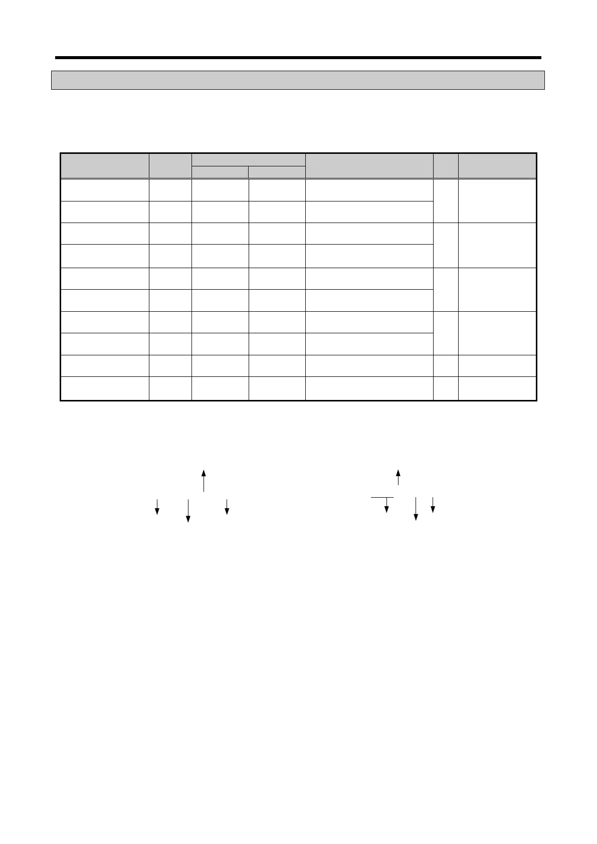
9.11.1 Data I/O area
Describes data I/O area
Variable name Type
Description R/W
_0y_ERR BIT U0y.00.0 %UX0.y.0 Module Error
R Option → CPU
_0y_RDY BIT U0y.00.F %UX0.y.15 Module Ready
_0y_DA0_ACT BIT U0y.01.2 %UX0.y.16 CH0 active
R Option → CPU
_0y_DA1_ACT BIT U0y.01.3 %UX0.y.17 CH1 active
_0y_DA0_ERR BIT U0y.01.A %UX0.y.20 CH0 error
R Option → CPU
_0y_DA1_ERR BIT U0y.01.B %UX0.y.21 CH1 error
_0y_DA0_OUTEN BIT U0y.06.0 %UX0.y.24 CH0 output state setting
W Option ↔ CPU
_0y_DA1_OUTEN BIT U0y.06.1 %UX0.y.25 CH1 output state setting
_0y_DA0_DATA WORD U0y.07 %UW0.y.4 CH0 input value W Option ↔ CPU
_0y_DA1_DATA WORD U0y.08 %UW0.y.5 CH1 input value W Option ↔ CPU
- In the device allocation, the small letter ‘y’ is the No. of the slot where the module is installed.
- For example, to Write the ‘CH0 Output A/D Value’ of the analog module installed in the slot 9, write in
U09.07 (%UW0.9.7 for IEC types)
U 0 9 . 0 7
.
[ype]
.
[]
7
9 - 22