51
MC14094 (U3501,U3502)
MC14094B
13
14
15
16
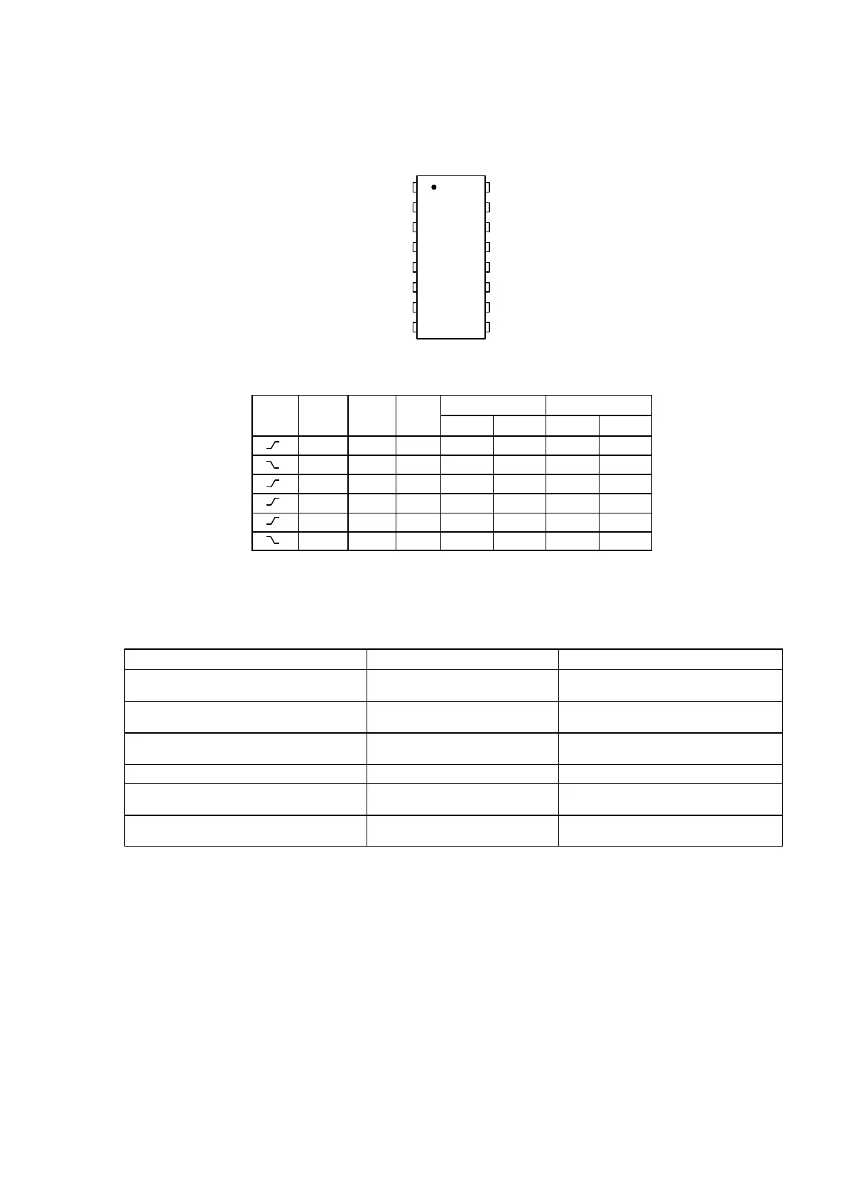
9
10
11
125
4
3
2
1
8
7
6
Q7
Q6
Q5
OUTPUT
ENABLE
V
DD
Q
S
Q′
S
Q8
Q1
CLOCK
DATA
STROBE
V
SS
Q4
Q3
Q2
PIN ASSIGNMENT
TRUTH TABLE
Clock
Output
Enable
Strobe Data
Parallel Outputs Serial Outputs
Q1 Q
N
Q
S
* Q′
S
0 X X Z Z Q7 No Chg.
0 X X Z Z No Chg. Q7
1 0 X No Chg. No Chg. Q7 No Chg.
1 1 0 0 Q
N
−1 Q7 No Chg.
1 1 1 1 Q
N
−1 Q7 No Chg.
1 1 1 No Chg. No Chg. No Chg. Q7
Z = High Impedance X = Don’t Care
* At the positive clock edge, information in the 7th shift register stage is transferred to Q8 and Q
S
.
ORDERING INFORMATION
Device Package Shipping
†
MC14094BCPG PDIP−16
(Pb−Free)
500 Units / Rail
MC14094BDG SOIC−16
(Pb−Free)
48 Units / Rail
MC14094BDR2G SOIC−16
(Pb−Free)
2500 Units / Tape & Reel
MC14094BDTR2G TSSOP−16* 2500 Units / Tape & Reel
MC14094BFG SOEIAJ−16
(Pb−Free)
50 Units / Rail
MC14094BFELG SOEIAJ−16
(Pb−Free)
2000 Units / Tape & Reel
†For information on tape and reel specifications, including part orientation and tape sizes, please refer to our Tape and Reel Packaging
Specifications Brochure, BRD8011/D.
*This package is inherently Pb−Free.
 Loading...