JTAG Programming
UG0451 User Guide Revision 7.0 14
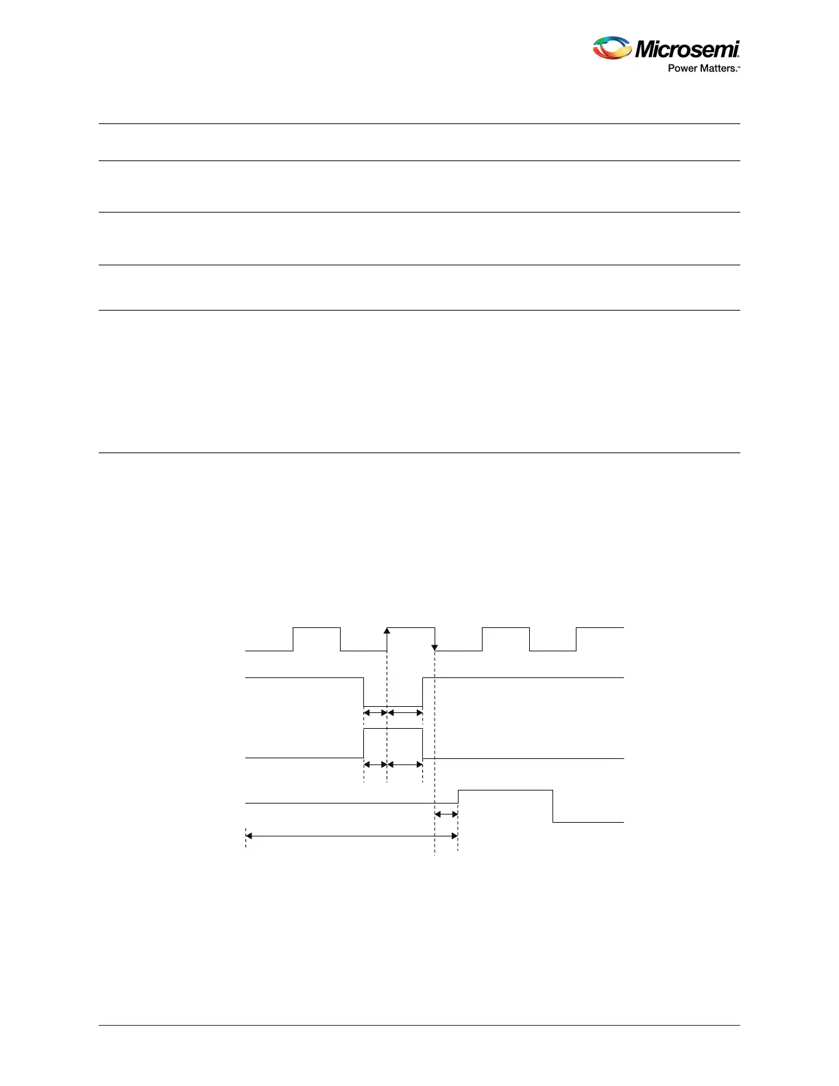
3.1.1 JTAG Timing Diagram
The following figure shows the JTAG signals timing diagram. The JTAG 1532 Timing Characteristics table
of the SmartFusion2 and IGLOO2 Datasheet specifies the timing numbers to be met to ensure proper
operation of the JTAG circuitry.
Figure 2 • JTAG Signals Timing Diagram
JTAG_TDI/
M3_TDI
1
Input Yes Not required Serial data input to JTAG boundary scan, UJTAG, and ISP.
UJTAG uses this pin or this pin aids another component to
use JTAG, ISP, and UJTAG.
JTAG_TDO/
M3_TDO
1
Output No Not required Serial data output from JTAG boundary scan, UJTAG, and
ISP. UJTAG uses this pin or this pin aids another component
to use JTAG, ISP, and UJTAG.
JTAG_TMS/
M3_TMS
1
Input Yes Not required The TMS pin controls the use of the following IEEE1532
boundary scan pins: TCK, TDI, TDO, and TRSTB.
JTAG_TRSTB/
M3_TRSTB
1
Input Yes Tie to GND
through 1 K
Reset pin for JTAG controller.
The TRSTB pin functions as an active low input to
asynchronously initialize or reset the boundary scan
circuitry. If JTAG is not used, an external pull-down resistor
can be included to ensure that the TAP is held in reset
mode. In critical applications, an upset in the JTAG circuit
could lead to an undesired JTAG state. In such cases,
Microsemi recommends tying off TRSTB to GND through a
resistor placed close to the FPGA pin.
1. Available only in SmartFusion2.
2. The UJTAG macro is a special purpose macro. It provides access to the user JTAG circuitry on-board the chip. You must
instantiate a UJTAG macro in the design to make use of the user JTAG feature. The TMS, TDI, TCK, TRSTB, and TDO pins of
the macro must be connected to the top-level ports of the design.
Table 6 • JTAG Pin Names and Description (continued)
Name Direction
Weak
Pull Up Termination Description
t
DISU
t
DIHD
t
TMSSU
t
TMSHD
TCK
TMS
TDI
TDO
t
TCK2Q
Tristate