Auto Programming
UG0451 User Guide Revision 7.0 22
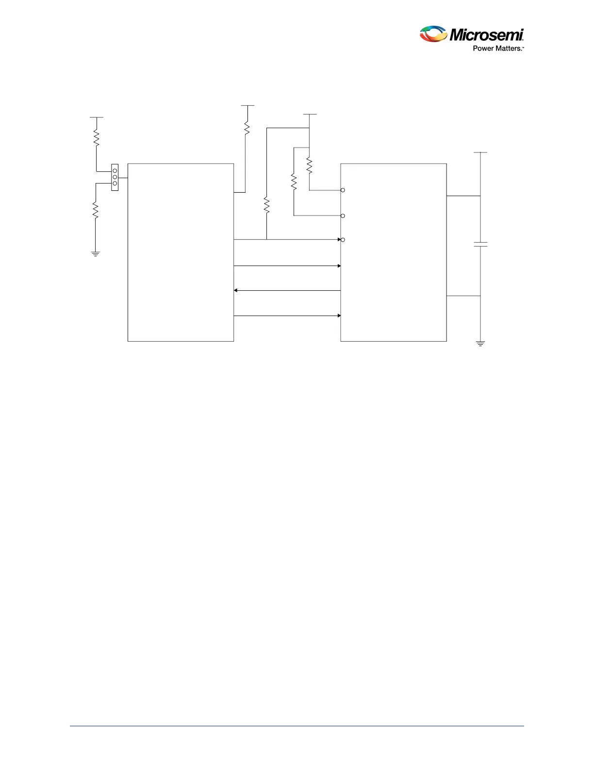
Figure 10 • SmartFusion2/IGLOO2 MSS/HPMS SPI_0 Port Configured for Auto Programming (Except 050
Device)
The MSS/HPMS SPI_0 port is enabled to operate as SPI master at power-on-reset when the
FLASH_GOLDEN_N pin is asserted low (pulled low with a 10 K resistor).
The FLASH_GOLDEN_N pin must be sensed by the system controller for a certain amount of time after
the DEVRST_N pin is deasserted or power-on-reset is completed. See the following figure for the timing
relations between power-on-reset and the FLASH_GOLDEN_N pin.
Figure 10, page 22 shows the control of the FLASH_GOLDEN_N pin using a three pin jumper. This pin
can be controlled by an external signal or a microprocessor.
Four SPI slave select pins of the SPI_0 interface (SS4, SS5, SS6, and SS7) drive high during auto
programing (except 005 and 010 devices). The remaining SPI_0 pins are tristated with weak pull up.
These four pins that drive high during auto programming must not be used as control pins.
The I/O level will be the same as bank voltage used for SPI_0 bank and the drive strength will be
maximum for this I/O level. For example, if the SPI_0 bank was powered by 1.8 V, then the drive strength
will be the maximum value allowed for 1.8 V LVCMOS I/O. For the maximum drive strength allowed for
LVCMOS 1.8 V transmitter, see the SmartFusion2 and IGLOO2 Datasheet.
The system controller reads the SPI flash device ID and device density to determine the read algorithm,
and then programs the device with the bitstream. In auto programming, SmartFusion2 and IGLOO2
devices are blank, and hence SPI signal polarity is mode 3 (SPO=SPH=1).
VDDIOy
3 Pin Jumper
10 K
10 K
10 K
10 K
10 K
3.3 V
3.3 V
0.1
µ
F
VPP
FLASH_GOLDEN_N
DEVRST_N
SPI_0_SDI
SPI_0_SDO
VCC
External Flash
SmartFusion2/IGLOO2
(Master)
DI
DO
GND
CLK
CS
HOLD
WP
SPI_0_CLK
SPI_0_SS0
y=bank number where
this pin is located
10 K