3 SIGNALS AND WIRING
3.6 Interface
93
3
Detailed explanation of interfaces
The details of I/O signal interfaces stated in the following section (refer to the I/O signal interface type in the table) are as
follows. Refer to the section and connect them with external devices.
Page 68 Signal (device) explanation
Digital input interface DI-1
This is an input circuit in which the photocoupler cathode side is the input terminal. Transmit signals from a sink (open-
collector) type transistor output, relay switch, etc. The following connection diagram is for sink input.
*1 For interfaces of the CN3-1 pin, CN3-10 pin, and CN3-19 pin of the MR-J5-_G_-RJ_, approximately 4.3 k.
For interfaces of the CN3-16 pin, CN3-45 pin, and CN3-50 pin of the MR-J5-_A_-RJ_, approximately 4.3 k.
For interfaces of the CN3-7 pin, CN3-9 pin, CN3-15 pin, and CN3-22 pin of the MR-J5W_-_G_, approximately 4.3 k.
*2 It is 500 mA for the MR-J5-_A_.
The following diagram is for when the CN3-10 pin and the CN3-35 pin are used as digital input interfaces.
Refer to the following for source input.
Page 97 Source I/O interface
TR
300 mA
*2
EM2
DICOM
± 10 %
V
CES
1.0 V
I
CEO
100 A
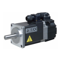
Servo amplifier
For transistor
Approx. 5 mA etc.
Approx. 6.2 k
*1
Switch
24 V DC
OPC
DOCOM
SD
V
CES
1.0 V
I
CEO
100 A
CN3-10, CN3-35
Approx. 1.2 k
Servo amplifier
24 V DC ± 10 %
500 mA
Approx. 20 mA
10 m or less

 Loading...