November 16, 2006 6881094C31-E
3-12 Theory of Operation: Transceiver Board
3.1.3.9.1 Power and Control
Since U104 is powered from switched B+, it makes its own regulated 4.5 Vdc to power the internal
logic. The supply input is V5EXT at pin 17, and the output is V45 at pin 16. RX at pin 23 is the control
signal to the antenna switch control circuit.
3.1.3.9.2 Voltage Multiplier
The PCIC contains an internal voltage multiplier. This multiplier produces signal V10 (pin 14), a 10-V
supply for the PCIC D/A converters (DACs). This enables the DACs outputs to reach 8 V. The FREF
signal is a 2.1 MHz clock used to switch the multiplier. The voltage multiplier is not used in either the
VHF, UHF Range 1, UHF Range 2, or 700–800 MHz radio.
3.1.3.9.3 Automatic Level Control (ALC)
In TX mode, the PCIC disables the receiver, turns on the transmitter, and controls the TX power
level. The automatic level control (ALC) circuit operates as follows:
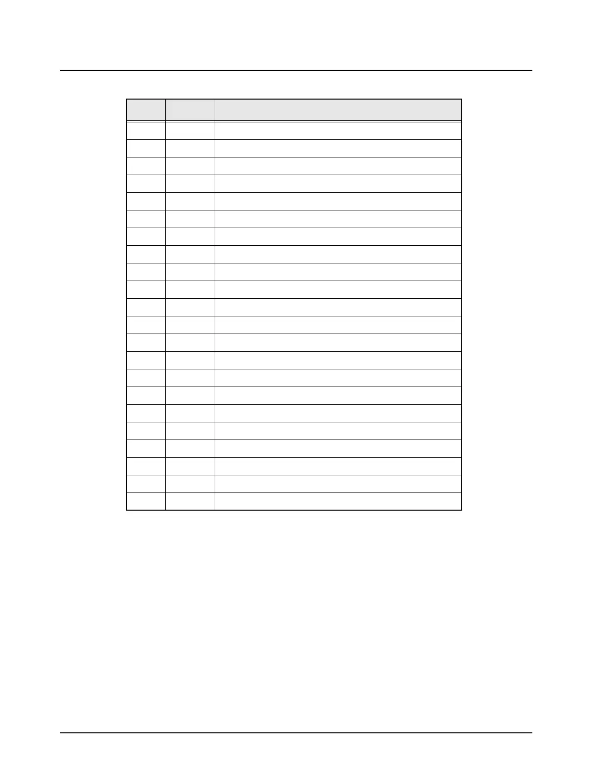
9 F168 Reference clock input, 2.1 MHz
10, 13 QX, CQX External capacitor for voltage multiplier
11, 12 Q, CQ External capacitor for voltage multiplier
14 V10 Voltage multiplier output
15 VG Internal band-gap reference voltage
16 V45 Regulated 4.5 Vdc output
17 V5EXT Power supply input for internal voltage regulator
18 VAR2 Buffered D/A output
19 VLIM Test point for internal D/A No.2 voltage
20 VAR1 Buffered D/A output
21 RS Asynchronous reset input
22 NA Spare pin
23 RX RX/TX mode control-bit output
24 VAR3 Buffered D/A output
25 GND2 Ground
26 CLK SPI clock input
27 BPOS Power supply input
28 DATA SPI data input/output
29 CEX SPI chip select input
30 TEMP Temperature sensor input
31 RSET External resistor; used to set the temperature cutback rate
32 ANO Switched BPOS output
Table 3-3. Power Control IC (U104) Pin Descriptions (Continued)
Pin Name Description

 Loading...