7- 10 M68000 8-/16-/32-BIT MICROPROCESSORS USER'S MANUAL MOTOROLA
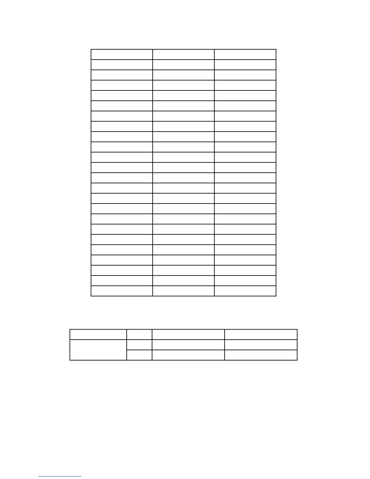
Table 7-13. Miscellaneous Instruction Execution Times
Instruction Register Memory
ANDI to CCR 32(6/0) —
ANDI to SR 32(6/0) —
EORI to CCR 32(6/0) —
EORI to SR 32(6/0) —
EXG 10(2/0) —
EXT 8(2/0) —
LINK 32(4/4) —
MOVE to CCR 18(4/0) 18(4/0)+
MOVE to SR 18(4/0) 18(4/0)+
MOVE from SR 10(2/0) 16(2/2)+
MOVE to USP 8(2/0) —
MOVE from USP 8(2/0) —
NOP 8(2/0) —
ORI to CCR 32(6/0) —
ORI to SR 32(6/0) —
RESET 136(2/0) —
RTE 40(10/0) —
RTR 40(10/0) —
RTS 32(8/0) —
STOP 4(0/0) —
SWAP 8(2/0) —
TRAPV (No Trap) 8(2/0) —
UNLK 24(6/0) —
+Add effective address calculation time for word operand.
Table 7-14. Move Peripheral Instruction Execution Times
Instruction Size Register → Memory Memory → Register
MOVEP Word 24(4/2) 24(6/0)
Long 32(4/4) 32(8/0)
+Add effective address calculation time.
7.12 EXCEPTION PROCESSING EXECUTION TIMES
Table 7-15 lists the timing data for exception processing. The numbers of clock periods
include the times for all stacking, the vector fetch, and the fetch of the first instruction of
the handler routine. The total number of clock periods, the number of read cycles, and the
number of write cycles are shown in the previously described format. The number of clock
Frees
cale Semiconductor,
I
Freescale Semiconductor, Inc.
For More Information On This Product,
Go to: www.freescale.com
nc...
 Loading...

